Moving LED Display Using MAX-6952 IC
SUMMARY
DESCRIPTION
BLOCK-DIAGRAM:

Fig. 1: Block Diagram of 8051 Microcontroller and MAX-6952 IC based LED Display
DESCRIPTION OF BLOCKS:
(1)8051 Microcontroller (AT89C51):
In this project I have used AT89C51 Microcontroller which is 40 pin µC. This µc has 4KB of ROM and 128 bytes of RAM and built in Timer/counter, UART modules etc. It has Total 32 I/O pins. It can run on any frequency between 4 to 44 MHz and I have used 12 MHz in this particular project.8051 micro-controller doesn’t have SPI module in it so I have used its i/o pin to interface with SPI compatible Max-6952 Display driver.
(2)MAX-6952 IC:
This Max-6952 IC can drive four single Colour matrix display or two bicolour matrix Display. It has total 40 pins. It can operate on 2.7V to5.5V.It included static RAM that stores each digit, as well as font data for 24user-definable characters and built-In ASCII 104-Character.This Max-6952 IC is SPI Compatible. It contains 16-bit shift register into which Input data are clocked on the rising edge of CLK, when CS is low. This IC have built-In ASCII 104 characters so to display any characters we have to just provide ASCII code in Hex to this IC through DIN (Data-Input) pin.

Fig. 2: Pin Diagram of Max-6952
O0 to O13: This pins are connected to LED display’s anode.
O14 to O23: This pins source current to the display’s anode columns.
V+: Positive Supply Voltage.
GND: Ground
DIN: Serial Data Input. Data is loaded into the internal 16-bit shift register on the rising edge of the CLK.
CLK: Serial-Clock Input. On the rising edge of CLK, data is shifted into the internal shift register. CLK input is active only while CS is low.
CS: Chip-Select Input. Serial data is loaded into the shift register while CS is low. The last 16 bits of serial data are latched on CS’s rising edge.
OSC: To use the internal oscillator, connect capacitor from OSC pin to GND pin. To use the external clock, drive OSC with a 1MHz to 8MHz CMOS clock.
Registers of Max-6952:
This IC has many registers but we need to configure at least four registers which are
1) Configuration Register,2) Scan Limit Register,3) Intensity Register,4) Data Register.
1) Configuration Register :

Fig. 3: Bit Values of Configuration Register
This register has total of bit from D0 to D7.Its address is 0x04.To configure this register we need to first shift address 0x04 into IC through DIN pin followed by data which need to configure as we need. We need to set or reset only two bits first is E bit and other one is S bit.E bit is Blink enable nit which is set to blink particular Digit. And S bit is use to select mode of operation 0 for shutdown mode and 1 for normal mode. Here we used normal mode and also blink disabled.
2) Scan-limit Register:
This register is used to select number of Digit we want to display either two or three. Its address is 0x03 and we need to set or reset only D0 bit to select between 2 or 4 Digit.0 for only two digits and 1 for all four.
3) Intensity Register:
This register is use to set intensity for individual digit. Here we set maximum intensity for better displaying. Its address is 0x01 for digit0 and digit 2 and 0x02 for digit1 and digit3.we need to load data 0x0f and 0xf0 means we need to set all four lower bits for digit0&2 and upper bits for digit1&3 to achieve maximum intensity.
4) Data Register:
This IC contains eight data registers to store the character data. These registers are arranged in two planes of 4 bytes, called P0 and P1 means each digit have two plan namely P0 & P1. Each digit is represented by 2 bytes of memory, 1 byte in plane P0and the other in plane P1.If we want to blink Display we just need to write data in one plan say P0 and leave plan P1 blank without data. If we don’t want to blink display we just need to write same data in both plans. But remember that to blink display we also need to enable blink mode using ‘E’ blink bit in configuration register.
METHOD TO INTERFACE IC-6952 WITH 8051
Serial-Data Format (16 Bits)

Fig. 4: Table Listing Serial Data Format for IC-6952
Above is given Serial-Data format to write data in to IC-Max-6952.To read or write data in this IC we first need to send read or write Bit means we need to inform IC whether we are going to read or write the data. After that we need to provide address where we want to write data. After address we need to send 8-Bit of data serially. All this bits must need to send serially.
Now to write data in to this IC we must need to follow some steps which is shown in flow diagram below.
First we need to make CS pin low which is chip select pin. Means we first need to select or activate chip. After this we need to provide rising edge of clock to send data or address in to shift register. First make CLK low and then send 1Bit of data/address then make CLK high. On each rising edge of clock 1 bit of data will be loaded in shift register. As we need to send total 16Bit of data which contain 1 read/write bit + 7Address bits + 8 data bits we need to repeat this step for 16 times. After sending 16 bit in to shift register we need to make CS pin High to latch 16bits of data from shift register to internal register of Max-6952.
Following are steps to write in to MAX-6952.

Fig. 4: Flowchart of C Code for 8051 Microcontroller and MAX-6952 IC based LED Display
Connection method for four single-color digits:

Fig. 5: Table Summarizing Connection Method for Four Single-Color Digits
This max-6852 IC has total 24 output pins (from O0 to O23) to drive four dot-matrix bar. Above is given connection method of this IC to Dot-matrix bar.O0 toO6 pins of IC is connected to Digit-0 and digit-1 means dot-matrix bar0 &1.Pin no.O7 to O13 of IC is connected to Digit-2 and digit-3.Now pin fromO14 to O18 is connected to Digit-0 and also to Digit-2.Pins fromO19 toO23 is connected to Digit-1 and Digit-3.
HOW IT WORKS:
The MAX6952 interfaced with AT89C51 through an SPI-compatible serial interface. The interface has three inputs, clock (CLK), chip-select (CS), and data in (DIN) and one output, data out (DOUT).Here in this project I have used only three input pins.
We need to configure four registers which are explained earlier. First we need to configure the configuration registers to select normal mode and blink disabled by loading address and data accordingly .We need to send write bit followed by address of configuration register and then data to sets the function. Then we need to set scan limit to select number of digit we want to us. Here we have used four digits so we need to load 0x01 data into scan limit register which has address 0x03.after that we have to set intensity of digit segments so here we set it to maximum using intensity register by loading data 0x0f and 0xf0 for digit0&2 and digit1&3 respectively. All this data must be loaded in to registers by using steps as I mentioned earlier.
After setting all this registers as per our requirement we need to provide data to data or digit register that we want to display. The data in the digit registers does not control the digits directly. Instead, the data means ASCII code is used to address a character generator, which stores the data of a 128-character font.
This IC have built-In ASCII 104 characters so to display any characters we have to just provide ASCII code in Hex to this IC through DIN (Data-Input) pin. We need to load ASCII code for individual digits into plan P0 and plan P1.If we need blinking mode then ASCII code need to be loaded in only one plan and other remains blank. If we don’t want blink mode we just need to write same ASCII in both plan. Here we are going to display ENGINEERS GARAGE without blinking so we need to write ASCII of all this characters in both plans. For example ASCII in hex of character E is 0x45 so we need to store 0x45 in data register of particular digit in both plans.
Here we are going to display message ENGINEERS GARAGE in scrolling manner which is achieved by shifting ASCII of particular character like we have only four digit segment so to display such long message we need to load ASCII of First four character in respective data register then need to shift ASCII of message one by one to achieve this pattern for example we need to write ASCII of “ENGI” into data register then after some delay we need to load ASCII of “NGIE” in to data register and so on. All this data must be loaded in steps as I mentioned. To load ASCII in particular digit we need to send address of that digit followed by ASCII code. Here we disabled the blinking mode so address of digit 0 to digit 3 is 0x60 to 0x63 respectively.
Project Source Code
###
//Program to #include <REGX51.H>sbit DIN=P2^0; //Data input Pin of MAX-6952sbit CLK=P2^2; //Clock pin of MAX-6952sbit CS=P2^1; //Chip select Pin of Max-6952//ASCII of characters in Hex//char A=0x41;char E=0x45;char N=0x4E;char G=0x47;char I=0x49;char R=0x52;char S=0x53;char space=0x20;//ASCII of characters in Hex//void init_max6952(void);void send(unsigned char value);void Send_AddrData(unsigned char Addr,unsigned char Data);void Send_A_D(unsigned char Addr,unsigned char Data);//delay//void delay(){unsigned int i;for(i=0;i<22000;i++);for(i=0;i<22000;i++);for(i=0;i<22000;i++);for(i=0;i<22000;i++);for(i=0;i<22000;i++);}void delay2(){unsigned int i;for(i=0;i<22000;i++);for(i=0;i<22000;i++);}void init_max6952() //function to initialize Max-6952{ Send_AddrData(0x04,0x01); //configuration register normal mode+Blink disabledSend_AddrData(0x03,0x01); //scan limit to 0-3Send_AddrData(0x01,0x0f); //maximum intensity for digit-0Send_AddrData(0x02,0x0f); //maximum intensity for digit-2Send_AddrData(0x01,0xf0); //maximum intensity digit-1Send_AddrData(0x02,0xf0); //maximum intensity digit-3}void led_data() //Function to display data{Send_AddrData(0x60,E); //data to digit register(address,data)Send_AddrData(0x61,N);Send_AddrData(0x62,G);Send_AddrData(0x63,I);delay();Send_AddrData(0x60,N);Send_AddrData(0x61,G);Send_AddrData(0x62,I);Send_AddrData(0x63,N);delay();Send_AddrData(0x60,G);Send_AddrData(0x61,I);Send_AddrData(0x62,N);Send_AddrData(0x63,E);delay();Send_AddrData(0x60,I);Send_AddrData(0x61,N);Send_AddrData(0x62,E);Send_AddrData(0x63,E);delay();Send_AddrData(0x60,N);Send_AddrData(0x61,E);Send_AddrData(0x62,E);Send_AddrData(0x63,R);delay();Send_AddrData(0x60,E);Send_AddrData(0x61,E);Send_AddrData(0x62,R);Send_AddrData(0x63,S);delay();Send_AddrData(0x60,E);Send_AddrData(0x61,R);Send_AddrData(0x62,S);Send_AddrData(0x63,space);delay();Send_AddrData(0x60,R);Send_AddrData(0x61,S);Send_AddrData(0x62,space);Send_AddrData(0x63,G);delay();Send_AddrData(0x60,S);Send_AddrData(0x61,space);Send_AddrData(0x62,G);Send_AddrData(0x63,A);delay();Send_AddrData(0x60,space);Send_AddrData(0x61,G);Send_AddrData(0x62,A);Send_AddrData(0x63,R);delay();Send_AddrData(0x60,G);Send_AddrData(0x61,A);Send_AddrData(0x62,R);Send_AddrData(0x63,A);delay();Send_AddrData(0x60,A);Send_AddrData(0x61,R);Send_AddrData(0x62,A);Send_AddrData(0x63,G);delay();Send_AddrData(0x60,R);Send_AddrData(0x61,A);Send_AddrData(0x62,G);Send_AddrData(0x63,space);delay();Send_AddrData(0x60,A);Send_AddrData(0x61,G);Send_AddrData(0x62,space);Send_AddrData(0x63,E);delay();Send_AddrData(0x60,G);Send_AddrData(0x61,space);Send_AddrData(0x62,E);Send_AddrData(0x63,N);delay();Send_AddrData(0x60,space);Send_AddrData(0x61,E);Send_AddrData(0x62,N);Send_AddrData(0x63,G);delay2();}void Send(unsigned char value){unsigned char i;for(i=0;i<8;i++){ CLK=0;//clock pin lowDIN=value&0x80; //1bit of data(MSB 1st) loaded in shift regestervalue=value<<1;CLK=1;//clock pin high}}void Send_AddrData(unsigned char Addr,unsigned char Data){CS= 0; //to select chipSend(Addr);//address of registersSend(Data);//dataCS=1; //CS high after 16bit}void main(){init_max6952();while(1){led_data(); //function to display messagedelay();}}
###
Circuit Diagrams
| Circuit-Diagram-8051-Microcontroller-MAX-6952-IC-LED-Display |  |
| Circuit-Diagram-8051-Microcontroller-MAX-6952-IC-LED-Display_0 | 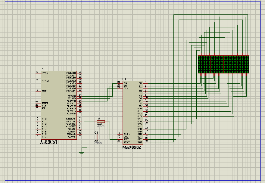 |
Project Video
Filed Under: Electronic Projects
Filed Under: Electronic Projects

Questions related to this article?
👉Ask and discuss on Electro-Tech-Online.com and EDAboard.com forums.
Tell Us What You Think!!
You must be logged in to post a comment.