Coin Toss/Flip Simulator Circuit

Summary

The Coin Flip Simulator is an interesting electronic project which can be used to conduct a toss between two teams or individuals. It is a decision maker used at the places where someone is not able to make up the mind. When a button is pressed, the head and tail LEDs start flashing alternatively at a high speed. The speed slows down and it finally stops with only one LED glowing which determines the final result.
This circuit is based on NE555 IC and 7473 one. Pin diagram of 7473 is shown below and details about NE555 can be found here
7473 IC

Description


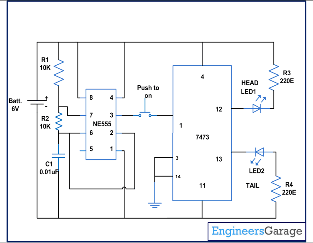
In this project 555 timer is wired in astable mode. 7473 IC contains two independent positive pulse triggered J-K flip-flops with complementary outputs.

The pin2 of the IC is for trigger input. When the voltage supplied to pin2 is less than 1/3 of the supply voltage, the output of the lower comparator forces the flip flop to have low logic state. This means output stage has reversing action. In other words, we can say that when output of the flip flop is LOW, the 555 timer’s output goes HIGH. Now if the power supply is first connected to astable circuit then initially the timing capacitor C1 is discharged. The voltage at pin2 becomes 0V and the output of timer is driven HIGH. Now C1 starts charging through R1 and R2. Capacitor C1 is also connected to pin6 which is threshold input of the timer.

 
When the pin1 (clock) of IC2 is LOW, no output is received. When clock is at positive transition, the data from J and K gets transferred from slave to the master. When the clock is at HIGH the J and K inputs become disabled and with negative transition the data from the master gets transferred to the slave.
 
When the switch S1 is pressed, Heads or Tails LED randomly gets selected. The maximum flash rate of the LED is about 2 KHz and pin2 of IC2 receives high. When the clock is HIGH, the logic states must not be allowed to change. Data gets transferred to the output at the falling edge of the clock pulse. The output can be reset by the low logic level on the clear input, regardless of the logic states at the other inputs.

Circuit Diagram

Components

You are here