Often people face problem while making a circuit on a bread board. It is a common problem that the circuit may work some time and may not work other time. Most of the time it is the connections on the bread board which creates this problem. Either are connections are not proper or loose or may get damaged while working or carrying the circuit on a bread board. Hence it is always recommended to make the circuit on a PCB once it has been tested on a bread board. But how to make a PCB at home? This article will explain the process of making a single layer PCB at home with the use of commonly available tools.
A printed circuit board has pre-designed copper tracks on a conducting sheet. The pre-defined tracks reduce the wiring thereby reducing the faults arising due to lose connections. One needs to simply place the components on the PCB and solder them.
Materials required in PCB Designing:
· Over Head Projector sheet (known as OHP sheets) or a wax paper.
· Laser Printer.
· Electric Iron.
· Steel wool.
· Two plastic trays.
· Copper board/ PCB (eg: paper phenolic, glass epoxy, FR4, FR10, etc.)
· Black permanent marker.
· Etching solution (Ferric chloride).
· Drill machine.
Step 1
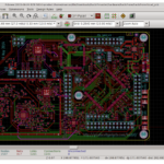
Step 1: Prepare a layout of the circuit on any commonly used PCB designing software. A layout is a design which interconnects the components according to the schematic diagram (circuit diagram). Take a mirror image print of the layout on the OHP sheet using a laser printer. Make sure that the design is correct with proper placement of the components.

Fig. 1: Image of mirror image print of the layout on the OHP sheet
Step 2
Step 2: Cut the copper board according to the size of layout. A copper board is the base of a PCB, it can be single layer, double layer or multi layer board.
Single layer copper board has copper on one side of the PCB, they are used to make single layer PCBs, it is widely used by hobbyist or in the small circuits. A double layer copper board consists of copper on both the sides of the PCB. These boards are generally used by the industries. A multilayer board has multiple layers of copper; they are quite costly and mainly used for complex circuitries like mother board of PC.

Fig. 2: Image of a double layer copper board
Step 3
Step 3: Rub the copper side of PCB using steel wool. This removes the top oxide layer of copper as well as the photo resists layer if any.

Fig. 3: Image showing copper side of PCB rubbed by steel wool
Step 4
Step 4: Place the OHP sheet (wax paper) which has the printed layout on the PCB sheet. Make sure that the printed/mirror side should be placed on the copper side of PCB.

Fig. 4: Image showing a white paper plaed over OHP sheet
Step 5
Step 5: Put a white paper on the OHP sheet and start ironing. The heat applied by the electric iron causes the ink of the traces on the OHP sheet to stick on the copper plate exactly in the same way it is printed on the OHP sheet. This means that the copper sheet will now have the layout of the PCB printed on it. Allow the PCB plate to cool down and slowly remove the OHP sheet. Since it is manual process it may happen that the layout doesn’t comes properly on PCB or some of the tracks are broken in between. Use the permanent marker and complete the tracks properly.

Fig. 5: Image showing OHP sheet ironed on copper side of PCB

Fig. 6: Image showing OHP sheet iron pressed on copper side of PCB

Fig. 7: Image showing removal of OHP sheet from PCB

Fig. 8: Image showing PCB Layout printed on copper side of PCB

Fig. 9: Image showing PCB Layout printed on copper side of PCB
Fig. 10: Image showing PCB Layout printed on copper side of PCB
Step 6
Step 6: Now the layout is printed on PCB. The area covered by ink is known as the masked area and the unwanted copper, not covered by the ink is known as unmasked area. Now make a solution of ferric chloride. Take a plastic box and fill it up with some water. Dissolve 2-3 tea spoon of ferric chloride power in the water. Dip the PCB into the Etching solution (Ferric chloride solution, Fecl3) for approximately 30 mins. The Fecl3 reacts with the unmasked copper and removes the unwanted copper from the PCB. This process is called as Etching. Use pliers to take out the PCB and check if the entire unmasked area has been etched or not. In case it is not etched leave it for some more time in the solution.

Fig. 11: Image showing PCB dipped in a solution of ferric chloride for etching
Step 7
Step 7: Take out the PCB wash it in cold water and remove the ink by rubbing it with steel wool. The remaining area which has not been etched is the conductive copper tracks which connect the components as per the circuit diagram.

Fig. 12: Image showing PCB after etching

Fig. 13: Image showing PCB cleaned by steel wool

Fig. 14: Image showing copper tracks printed on PCB
Step 8
Step 8: Now carefully drill the PCB using a drilling machine on the pads.

Fig. 15: Image showing holes drilled in PCB for placing components
Step 9
Step 9: Put the components in the correct holes and solder them.
This completes your PCB fabrication now put the components on mounting side and solder them. Make sure that you properly dispose of the FeCl3 solution, clean your tools and wash your hands after this exercise. You can also store the solution in a plastic box for future use but not for too long.
You may also like:
Filed Under: Tutorials

Questions related to this article?
👉Ask and discuss on Electro-Tech-Online.com and EDAboard.com forums.
Tell Us What You Think!!
You must be logged in to post a comment.