In our previous experiment, we designed the 5V converter by AP65111AWU-7 SMD IC. In this experiment, we will explore a new IC for converting 12V to 5V DC and then compare both of the IC’s performance curves.
We will take an adjustable LM2576 switching regulator, a buck regulator with a fixed frequency of 52 kHz. The IC can provide a maximum output current of 3A.
Note: To get in-depth information of dc-dc to buck converter and how it works, please refer to our previous series on SMPS.
Basic design
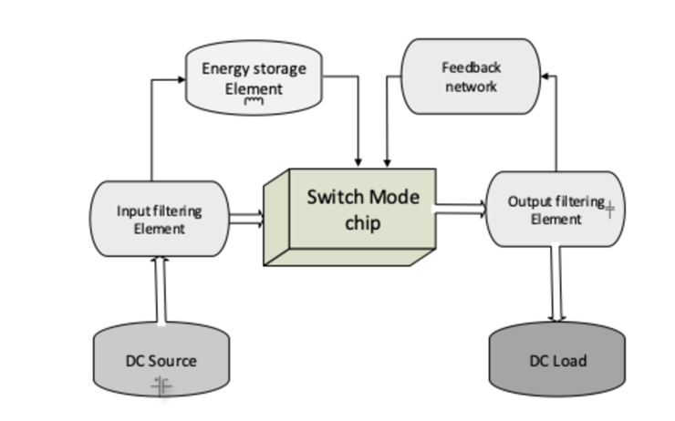
Basic principle
The switch mode IC works on the principle of power conversion and switching mechanism. They try to maintain equal input and output power, but due to losses in the components between circuits, the efficiency of these ICs does not reach 100%. However, they are more efficient than linear ones, which dissipate a lot of power in terms of heat.
We can also design a switch mode regulator without using any switch mode IC by discrete component, as we have designed in our previous series.
Components
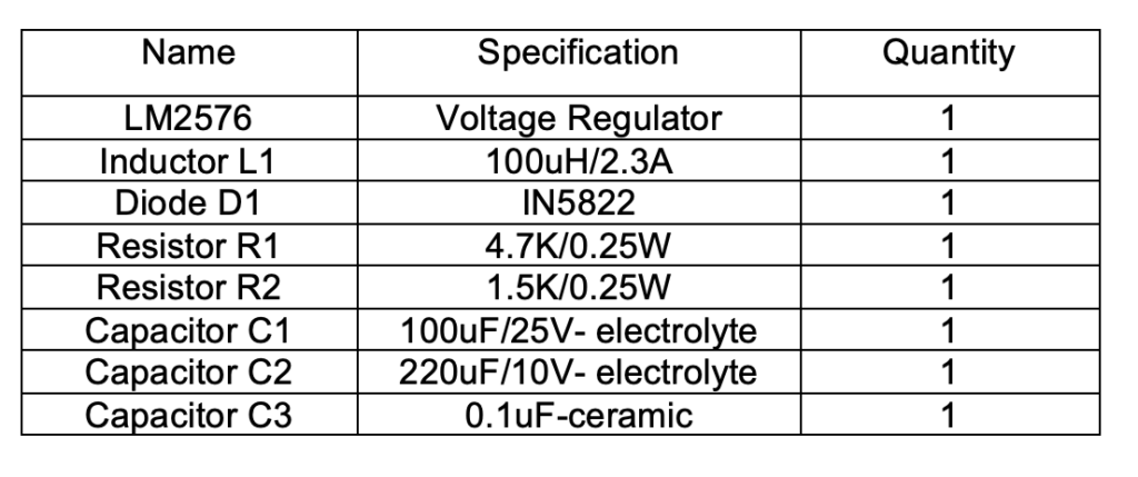
Below are the parts that we have used in our design.
Circuit Diagram
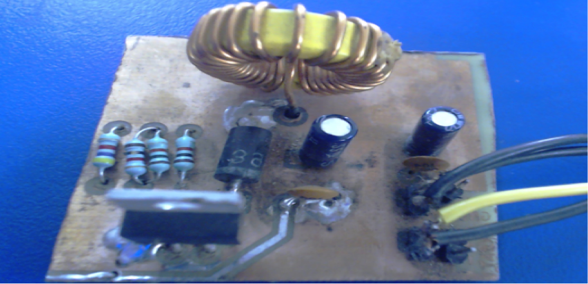
Building the circuit
The LM2576 internally has a switching mechanism and error amplifier, which maintains the output voltage. Apart from this, we want the following external components for its design.
Inductor and diode
These are the basic needs of the circuit; the inductor work is to store the energy in the form of a magnetic field, and on the other hand, the diode acts as a switch that completes the switching cycle.
Inductor selection
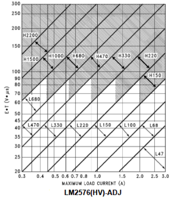
The below graph can use to find the suitable inductor for our application. This graph is in the IC datasheet, which needs output current and E*T (V.us) for inductor value calculation.
Step 1: The following equation can be used for the calculation of the above values
E*T = (Vin-Vout)*(Vout/Vin)*(1000/F(in kHz)) V. us
Desired Parameters
Vout = 5V, Vin = 12V, F = 52kHz
After putting all the values, we get
E*T = 55.7 V.us
Step 2: Selecting Output current = 2A
Step 3: For an output current of 2A and ET value of 56 Vus, we can see the intersected part in the graph and choose the inductor. For our application, we get an inductor of 100uH from the graph, and the current rating of the inductor should be 1.15 times the output load current.
That results in L = 100uH/2.3A
IN/OUT capacitors
The input and output capacitor helps out in the filtering of any high voltage spike. Also, the output capacitor plays a vital role in the off period of the switching cycle and provides sufficient energy for the regulated output voltage.
Feedback network
For the desired voltage at the output, we need a resistor divider network that will feed the output voltage to the feedback pin. The internal error amplifier proceeds this signal and maintains a regulated voltage at the output.
Selecting feedback network
The following equation calculates the value of the resistor divider
Vout = Vref(1+R1/R2)
Vref = 1.23V, IC reference voltage
For Vout = 5V
We can take,
R1 = 4.7K and R2 = 1.5k
Practical observation
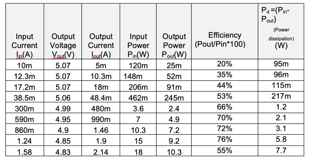
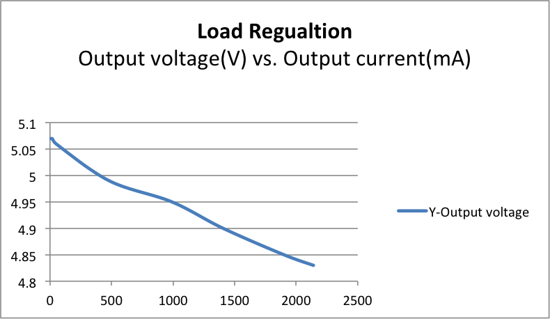
Vin, Input voltage = 12V, Vout(without load) = 5.07V
Thermal management
Every component has its operating temperature range. To keep the temperature below its operational limits, heat sink and cooling fans are used, and sometimes TEC (thermoelectric cooler) is also used.
Please refer to our article “Power Supply Thermal Management” to learn about the selection parameters of a heat sink or cooling fan.
Precautions
- A capacitor should be connected between IN pin and the ground to keep the DC input voltage regulated.
- The circuit’s capacitor must have a higher voltage rating than the input supply voltage. Otherwise, the capacitor starts leaking the current due to the excess voltage at its plates and will burst out.
- Ensure all the capacitors are discharged before working on a DC power supply.
- The current rating of the inductor should be 1.15 times greater than the output current.
- Do not give a higher voltage at input than the IC operating input voltage range.
- Do not short the output terminals; this will reverse the current flow in the IC, and the IC will get faulty.
- Also, do not short the input terminals; this will generate a large current in the circuit, and the components in the circuit get faulty.
- Frequency effect
The higher the frequency of the IC, the higher the switching losses, which decreases the efficiency. But high switching frequency reduces the size of the energy storage element and improves the transient response.
PCB design guidelines
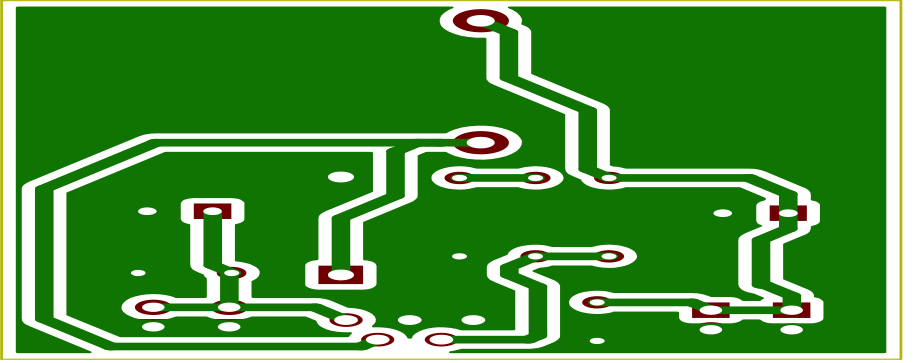
- Keep power traces thick and short.
- Place the input and output capacitor as close as the input and output pin of the IC.
- Minimize the path length of the inductor and diode.
- Keep voltage and switching nodes away from each other.
Comparison between LM2576 and AP65111AWU
We made a 12V to 5V buck converter in our previous designs with AP65111AWU (SMD). As pit’she availability, we have taken one IC in the through-hole packageapplication’sIC in the SMT package. Now it’s time to compare both so that one can select the best IC per the application’s need.
You may also like:
Filed Under: Tutorials








Questions related to this article?
👉Ask and discuss on EDAboard.com and Electro-Tech-Online.com forums.
Tell Us What You Think!!
You must be logged in to post a comment.