An inverter is a device which converts Mains (AC Supply) to DC and charge the battery when Mains is available and converts back DC from battery to AC supply when supply of Mains is not there. It is now become a very important part of Indian houses.
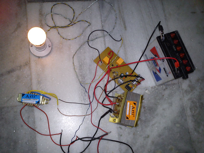
Material Required
1. Zero PCB
2. Heat Sink
3. Connectors
4. Connecting Wires
5. Transistors
a. TIP 3055
b. BC547
6. Diode – 1N4007
7. IC’s
a. HCF 4047BE
b. LM317
8. Resistors
a. 470 Ohm
b. 100 Ohm
c. 120 Ohm
d. 820 Ohm
e. 10 k Ohm
f. 1.5 k Ohm
g. 3.3 k Ohm
9. Capacitors
a. 220nF
b. 100uF
c. 470uF
10. Potentiometers
a. 47 k Ohm
b. 500 Ohm
11. Relays
12. Transformers
a. 9-0-9 (1 A)
b. 12-0-12 (5A)
Working
Working
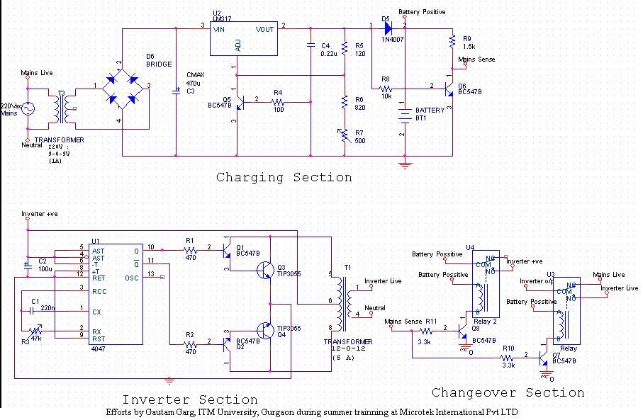
Charging
When Mains is there we will get 220V AC. 9-0-9 Transformer will converter it into 18V AC. Then Bridge Rectifier will rectify it. 470uF capacitor is installed in parallel to it to filter it. Then LM317, which is a voltage regulator IC, will convert the voltage to desired voltage for charging. 500 Ohm potentiometer is there which will be used to adjust the voltage to desired value. Then a protecting diode (D5) is there which will prevent the backflow of the current when there will no Mains. Hence we will connect battery to charge it.
Discharging
The heart of the discharging circuit is a HCF4047 IC which is wired as an astable multi vibrator here. Resistance and Capacitance at pin 1&2 determines the output frequency. Here it is set to 50Hz. Due to this a two 180 degree out of phase, 50 Hz, 50% duty cycle waveforms will appear at pin 10 & 11. Then these waves are amplified by the Darlington pair configuration of BC547 and TIP 3055. Then outputs from both amplified waves are given to step-up transform (12-0-12 to 220). Hence, we get 220V AC supply that is converted from 12V DC from the battery.
Change Over Section
Function of change over section is to switch on the inverter and shift the output to the external Appliances from Mains to inverter, when Mains is not there. This changing is generally performed with the help of Relays.
Charging Section (before protecting diode), is also act as Mains sense circuit. So, when Mains is not there, we have to energies the relays to shift it to the inverter mode. Hence for these task a NOT Gate is there to perform this task.
Then two BC547 transistors are there to drive the relays. 1st relay switches between Mains and inverter output. And 2nd switches on the DC to AC conversion or Discharging section when Mains is not there.
Specifications
|
|
DC A
|
DC V (Battery)
|
Charging Voltage
|
I/P V
|
I/P A
|
I/P W
|
PF
|
|
Charging
|
0.3
|
12.7
|
13.83
|
232.3
|
0.064
|
13.9
|
0.919
|
|
Discharging
|
DC A
|
DC V
|
O/P V
|
O/P A
|
O/P W
|
O/P PF
|
|
No Load
|
0.64
|
12.5
|
219.2
|
–
|
–
|
–
|
|
40W Load
|
3.05
|
12.25
|
152.8
|
0.147
|
22.4
|
1.00
|
Load: 40W
Delay Time
1. Mains to Inverter Mode: 1750ms
2. Inverter Mode to Main: 10ms
Graphs
Graphs
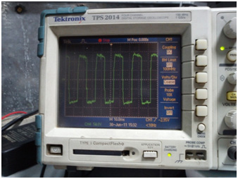
Inverter Mode Output
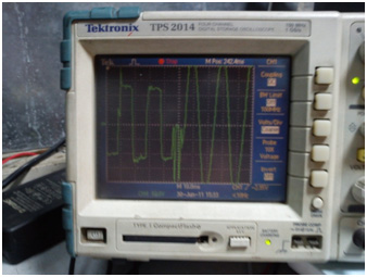
Inverter to Mains
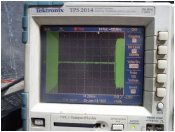
Mains to Inverter Mode
Project Source Code
Circuit Diagrams
Filed Under: Electronic Projects

Questions related to this article?
👉Ask and discuss on EDAboard.com and Electro-Tech-Online.com forums.
Tell Us What You Think!!
You must be logged in to post a comment.