IC 555 timer is a well-known component in the electronic circles but what is not known to most of the people is the internal circuitry of the IC and the function of various pins present there in the IC. Let me tell you a fact about why 555 timer is called so, the timer got its name from the three 5 kilo-ohm resistor in series employed in the internal circuit of the IC.
IC 555 timer is a one of the most widely used IC in electronics and is used in various electronic circuits for its robust and stable properties. It works as square-wave form generator with duty cycle varying from 50% to 100%, Oscillator and can also provide time delay in circuits. The 555 timer got its name from the three 5k ohm resistor connected in a voltage-divider pattern which is shown in the figure below. A simplified diagram of the internal circuit is given below for better understanding as the full internal circuit consists of over more than 16 resistors, 20 transistors, 2 diodes, a flip-flop and many other circuit components.
The 555 timer comes as 8 pin DIP (Dual In-line Package) device. There is also a 556 dual version of 555 timer which consists of two complete 555 timers in 14 DIP and a 558 quadruple timer which is consisting of four 555 timer in one IC and is available as a 16 pin DIP in the market.
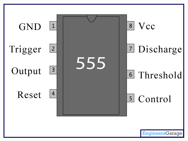
Fig. 1: Pin Diagram of 555 IC
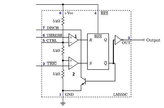
Fig. 2: Internal Circuit Diagram of 555 IC
Basics Concepts:
· Comparator: The Comparator are the basic electronic component which compares the two input voltages i.e. between the inverting (-) and the non-inverting (+) input and if the non-inverting input is more than the inverting input then the output of the comparator is high. Also the input resistance of an ideal comparator is infinite.
· Voltage Divider: As we know that the input resistance of the comparators is infinite hence the input voltage is divided equally between the three resistors. The value being Vin/3 across each resistor.
· Flip/Flop: Flip/Flop is a memory element of Digital-electronics. The output (Q) of the flip/flop is ‘high’ if the input at ‘S’ terminal is ‘high’ and ‘R’ is at ‘Low’ and the output (Q) is ‘low’ when the input at ‘S’ is ‘low’ and at ‘R’ is high.
Function of different Pins:-
1. Ground: This pin is used to provide a zero voltage rail to the Integrated circuit to divide the supply potential between the three resistors shown in the diagram.
2. Trigger: As we can see that the voltage at the non-inverting end of the comparator is Vin/3, so if the trigger input is used to set the output of the F/F to ‘high’ state by applying a voltage equal to or less than Vin/3 or any negative pulse, as the voltage at the non-inverting end of the comparator is Vin/3.
3. Output: It is the output pin of the IC, connected to the Q’ (Q-bar) of the F/F with an inverter in between as show in the figure.
4. Reset: This pin is used to reset the output of the F/F regardless of the initial condition of the F/F and also it is an active low Pin so it connected to ‘high’ state to avoid any noise interference, unless a reset operation is required. So most of the time it is connected to the Supply voltage as shown in the figure.
5. Control Voltage: As we can see that the pin 5 is connected to the inverting input having a voltage level of (2/3) Vin. It is used to override the inverting voltage to change the width of the output signal irrespective of the RC timing network.
6. Threshold: The pin is connected to the non-inverting input of the first comparator. The output of the comparator will be high when the threshold voltage will be more than (2/3) Vin thus resetting the output (Q) of the F/F from ‘high’ to ‘low’.
7. Discharge: This pin is used to discharge the timing capacitors (capacitors involved in the external circuit to make the IC behave as a square wave generator) to ground when the output of Pin 3 is switched to ‘low’.
8. Supply: This pin is used to provide the IC with the supply voltage for the functioning and carrying of the different operations to be fulfilled with the 555 timer.
Uses:-
The IC 55 timer is used in many circuits, for example One-shot pulse generator in Monostable mode as an Oscillator in Astable Mode or in Bistable mode to produce a flip/flop type action. It is also used in many types of other circuit for achievement of various purposes for instance Pulse Amplitude Modulatin (PAM), Pulse Width Modulation (PWM) etc.
More about these circuits will be explained in the later tutorials.
Exploring the Datasheet
We may have used 555 Timer IC in one or more applications like oscillator, timer, PWM etc. We may have seen IC 555 in most of the applications. But most of us do not know how these 555 timer circuits are designed. How IC555 is used in such applications. To design IC555 based applications one should first refer its datasheet. It provides all the related information about the chip. It provides pin diagram, pin functions, working, operations, and most important its various operating parameters like rated supply voltage and current, high output voltage, low output voltage, sinking current-sourcing current capacity, operating temperature etc so many. After referring to all these, one may be able to design its own application using IC555 or may be able to use IC555 in proper manner.
So here I am going to explain some of the operating parameters of IC555 that will tell you to use IC555 in proper manner. For all given parameters I have taken reference of LM555 /NE555/SA555 datasheet provided by “Fairchild semiconductor”.
|
parameter |
condition |
Min value |
Max value |
Explanation |
|
Supply voltage (Vcc) |
|
4.5 V |
16 V |
The biasing voltage limit should not exceed these two limits |
|
Supply current (Icc) |
Vcc = 5V & RL = ? |
|
6 mA |
For 5V supply and output open circuited the maximum supply current is limited to 6 mA |
|
Power dissipation (PD) |
|
|
600 mW |
When IC555 is in running condition it dissipates 600 mW |
|
Operating temperature |
|
0oC |
70oC |
IC555 should be operated within this temperature range. Beyond it performance will deteriorate |
|
Soldering temperature |
For 10 sec |
|
300oC |
If IC555 is directly soldered in circuit the maximum soldering temperature should not exceed 300 oC |
|
Storage temperature |
|
-65 oC |
150 oC |
IC555 should not be stored beyond these storage temperature limits |
|
Control voltage (Vc) |
Vcc = 5 V |
2.6 V |
4 V |
The input voltage at pin number 5 is limited to 2.6 V to 4 V for 5 V supply |
|
Threshold voltage (Vth) |
Vcc = 5 V |
3.33 V |
3.33 V |
The input voltage at pin number 6 should be slightly higher than this value |
|
Trigger voltage (Vtr) |
Vcc = 5 V |
1.1 V |
2.2 V |
The input voltage at pin number 2 must be less than 2.2 V for 5 V supply. Its typical value is 1.67 V |
|
Reset Voltage (Vrst) |
|
0.4 V |
1 V |
The reset input voltage at pin number 4 should be higher than 0.4 V for proper operation |
|
Threshold current (Ith ) |
Vcc = 5 V |
|
0.25 µA |
This current will limit the value of total resistance (R1+R2) = 6.7 M? |
|
Trigger current (Itr) |
Vtr = 0 V |
|
2 µA |
The trigger input requires maximum 2 µA current |
|
Reset current (Irst) |
|
|
0.4 mA |
|
|
Low output voltage (Vol) |
Vcc = 5 V Isink = 5 mA |
0 V |
0.35 V |
For 5 V supply the maximum output low voltage is 0.35 V |
|
High output voltage (Voh) |
Vcc = 5 V Isource = 100 mA |
2.75 V |
Vcc |
For 5 V supply the minimum output high voltage is 2.75 V |
|
Sinking current (Isink ) |
Vcc = 5 V |
|
5 mA |
For 15 V supply when output is low chip can maximum sink 50 mA current from supply |
|
Vcc = 15 V |
10 mA |
50 mA |
||
|
Sourcing current(Isource) |
Vcc = 5 V |
|
100 mA |
For 15 V supply when output is high chip can maximum source 200 mA current to load |
|
Vcc = 15 V |
100 mA |
200 mA |
||
|
Rise time (Tr) |
|
|
100 nS |
Time required for output to rise from low value to 50 % of maximum value is 100 n sec only |
|
Fall time (Tf) |
|
|
100 nS |
Time required for output to fall from high value to 50 % is 100 n sec only |
Basics of 555 Timer IC
Multivibrators find their own place in many of the applications as they are one of the most widely used circuits. The application may be household (domestic), industrial, access control, communication etc anyone. The multivibrators are used in all such applications as oscillators, as digital flip-flop, as pulse generator circuit, as delay generator circuit, as a timer and many more.
There are three types of multivibrators
1. Astable multivibrator – it has no stable state. It has two quasi stable states that automatically changes from one to another and back. So actually it changes from high to low state and low to high state without any trigger input after pre determine time.
{ 2. Monostable multivibrator – it has one stable state and one quasi stable state. It jumps into quasi stable state from stable state when trigger input is applied. It comes into stable state from quasi stable state after pre determine time automatically.
3. Bistable multivibrator – it has both stable states. Two different trigger inputs are applied to change the state from high to low and low to high.
All these three kinds of multivibrators can be easily made using transistors. But one IC is available that can be used as astable, monostable or bistable multivibrator and that is IC555.
IC 555 is the most versatile chip and it is (can be) used in all most every kind of application because of its multi functionality. Its 8 pin DIP or SOP package type chip with 200 mA direct current drive output. It’s called mixed signal chip because there are analog as well as digital components inside. Its main applications are to generate timings, clock waveform, generate synchronizing signals, square wave oscillator, in sequential circuit and many more.
Pin diagram, pin details and pin functions

Fig. 3: Pin Diagram of 555 IC
|
Pin no |
Pin name |
I / O |
function |
|
1 |
Gnd |
input |
Provides ground |
|
2 |
Trigger |
input |
Trigger comparator input pin. Negative trigger (< 1/3 Vcc) is applied in monostable operation |
|
3 |
Output |
output |
Its output pin |
|
4 |
Reset |
input |
Internal flip flop reset pin. Must be high to enable output |
|
5 |
Control |
input |
Control voltage input to control charging discharging of external capacitor |
|
6 |
Threshold |
input |
Threshold comparator input pin. Positive trigger (>2/3 Vcc) is applied in bistable operation |
|
7 |
Discharge |
input |
Discharge pin. Provides discharge path to external capacitor |
|
8 |
Vcc |
input |
For +Ve biasing voltage. Between 4.5 V to 16 V |
Internal block diagram –

Fig. 4: Block Diagram of 555 IC
As shown in figure IC555 includes two comparators, one RS flip-flop and other few discrete components like transistors, resistors etc. the biasing voltage (Vcc) is divided in three parts through voltage divider using same value of resistors R. from these 1/3 Vcc is given to non inverting terminal of trigger comparator and 2/3 Vcc is given to inverting terminal of threshold comparator. The outputs of both comparators are given to R and S inputs of flip-flop. The Q’ output is actual output of IC and Q output drives discharging transistor that provides discharging path to external capacitor whenever it is high.
When negative trigger <1/3 Vcc is applied at trigger input pin, the trigger comparator gives high output that resets the flip flop and Q’ output that is the output of chip goes high.When positive trigger >2/3 Vcc is applied at threshold input pin, the threshold comparator gives high output that sets the flip flop. The Q output will become high and the output of chip goes low. At that time discharging transistor that provides discharging path to external capacitor.The high reset input keeps flip-flop enable. If it is low, flip-flop disables and output will be low. No any effect of threshold and trigger comparator outputs.
Understanding Operating Modes
IC555 operating modes
IC555 has three different operating modes. These operating modes actually correspond to three different multivibrator configurations.
1. Astable mode – it is also known as self triggering or free running mode. It has no stable state. It has two quasi stable states that automatically changes from one to another. It changes from high to low state and low to high state without any trigger input after pre determine time. This mode is used to generate square wave oscillations, clock pulse, PWM wave etc.
2. Monostable mode – it is also known as single shot mode. It has one stable state and one quasi stable state. It jumps into quasi stable state from stable state when trigger input is applied and comes back to stable state after pre determine time automatically. It is used in generating pulses, time delay etc.
3. Bistable mode – it is also known as flip-flop mode. It has both stable states. Two different trigger inputs are applied to change the state from high to low and low to high. It is used in automatic switching applications, to generate pulse of variable time etc.
Astable mode

Fig. 5: Circuit Diagram of 555 IC in Astable Mode
The above figure illustrates the connections of IC555 used as astable multivibrator.
Connections: – resistance R1 is connected between Vcc pin (no. 8) and discharge pin (no. 7). Another resistance R2 is connected between threshold pin (no. 6) and discharge pin. Trigger pin (no. 2) is shorted with threshold pin. Capacitor C is connected as shown between threshold pin and ground. Control voltage input pin (no. 5) is connected to ground through 0.1µF capacitor. The output is taken from pin no. 3. Reset input pin (no. 4) is connected to Vcc to enable internal flip-flop operation. Pin no. 8 is connected to Vcc for +Ve bias and pin no. 1 is connected to ground for –Ve bias.
Operation: – as we know already, this mode is self triggering and changes its state automatically from high to low and low and high. This is achieved by shorting threshold and trigger pin. The output waveform is also shown in figure.
· Initially output is high. The capacitor charges towards Vcc through R1 and R2
· When it reaches 2/3 Vcc, the threshold comparator gives high output. This will set the flip-flop. So the output becomes low and discharging transistor becomes ON.
· So capacitor finds discharging path through R2 to discharge pin.
· As capacitor discharges to 1/3 Vcc, the trigger comparator gives high output. This will reset the flip-flop. So output again becomes high and discharging transistor is OFF.
· So capacitor will again start charging.
· Thus capacitor will charge and discharge between 2/3 Vcc and 1/3 Vcc limits. This cycle continuous and we get high-low-high-low output continuously at a rate of charging and discharging of capacitor.
Design Equations: –
The capacitor charges to Vcc through resistors R1 and R2. So charging time is given by
T1 = (R1 + R2)×C × ln 2
During this time the output is high so we can write
TH = (R1 + R2)×C × ln 2 = 0.693×(R1 + R2)×C
In discharging path only resistance R2 comes into picture. So discharging time is given by
T2 = R2×C ×ln 2
During this time the output is low so we can write
TL = R2×C× ln 2 = 0.693×R2×C
But total time is
TT = TH + TL
= 0.693×(R1 + R2)×C + 0.693×R2×C
= 0.693×(R1 + 2×R2)×C
And because frequency is inverse of time so
F = 1 / /TT = 1 / 0.693×(R1 + 2×R2)×C
That means
Frequency = 1.44 / (R1 + 2×R2)×C ___________________(I)
The duty cycle is given by
Duty cycle = on time / total time %
= 0.693×(R1 + R2)×C / 0.693×(R1 + 2×R2)×C
Duty cycle = (R1 + R2) / (R1 + 2×R2) % ______________(II)
Equations (I) and (II) are design equations for astable multivibrator using IC555. Using these two equations one can find out the values of R1, R2 and C. How this is done is explained in next tutorial.
Astable mode for 50% (or less) duty cycle: –
Now one problem in connecting astable multivibrator in above manner is, we will get duty cycle more than 50%. It is not possible to design it for less than 50% because
Duty cycle = (R1 + R2) / (R1 + 2×R2) %
In this equation if you exclude R1 (by assuming R1=0) then you will get
Duty cycle = R2 / 2×R2 % = 50%
But we can not make R1 = 0 in above circuit. That’s why an exact 50% duty cycle or less than that is not possible.
So what can be done to get exact 50% (or less) duty cycle?
The answer is to use one simple diode. Here is the circuit.

Fig. 6: Circuit Diagram of 555 IC in Astable Mode for 50% Duty Cycle
As shown in above figure one diode is connected in forward direction accors resistance R2. In the circuit now instead of using two different value resistors, only one value (R) is used as R1 and R2.
The operation of circuit is simple. Initially output is high and capacitor charges to 2/3 Vcc through upper resistor. At this time output becomes low. Then capacitor discharges to 1/3 Vcc through lower resistor. Because both resistance values are same we shall get same charging time and discharging time that means exact 50% duty cycle.
To find out equation of frequency, the capacitor charging time for which output is high is given by
TH = R×C × ln 2 = 0.693×R×C
Simillarly the capacitor discharging time for which output is low
TL = R×C × ln 2 = 0.693×R×C
Now because total time is
TT = TH + TL
= 2× TH (or 2×TL)
= 2×0.693×R×C
= 1.368×R×C
And frequency is given by
F = 1/ TT = 1 / (1.368×R×C)
F = 0.72 / RC
Now to decrease the duty cycle furthur (less than 50%) one has to reduce the value of upper resistance (R1) than lower resistance (R2). This will decrease charging time. So the ON time (high output time) is decreased and duty cycle also decreases. To increase duty cycle completely reverse has to be done. To vary the duty cycle from minimum to maximum one can use potentoimeter instead of fixed value resistors (at either R1 or R2). One of such possible circuit with all component values is shown here.

Fig. 7: Circuit Diagram of 555 IC in Astable Mode for 50% Duty Cycle
Note: – the output of this circuit is called PWM (pulse width modulated) output. It is widely used for speed conntrol of DC motors.
Astable mode to generate PWM output at constant frequency: –
The problem in above PWM circuit is, its output frequency will also change as the output width changes. The output frequency is inversely propotional to the value of resistance. So as resistance is increased or decreased, the frequency is decreased or increased.
So what should be done to keep the output frequency constant or fixed?
The answer is again to use diode. This time not just one but two diodes. The circuit is as shown below.

Fig. 8: Circuit Diagram of 555 IC in Astable Mode generating PWM Output
Connections: – the two diodes are connected back to back with two terminals of 10K potentiometer with discharge pin as shown. The slider pin is connected with 1 µF capacitor and threshold pin. Rest of the connections are similar.
Operation: – as I said earlier to keep frequency constant the total resistance must be kept constant. This is done with the help of two diodes
When output is high, the capacitor charges through 1K, D1 and part of 10K resistor (say R1) and reaches to 2/3 Vcc
The output goes low and now capacitor discharges through another part of 10K (say R2) and D2 to 1/3 Vcc
So by sliding 10K pot left side R1 decreases – charging time decreases – ON time decreases – duty cycle decreases. But at the same time R2 increases – discharging time increases – OFF time increases
Similar to that if pot is turned right side, R1 increases – charging time increases – ON time increses – duty cycle increases. But because R2 is decreased, OFF time is decreased
Thus by sliding pot on both side the ON time and OFF time increases / decreases but total time remains constant and that’s why frequency also remains constant. The waveforms are as shown in figure.
Monostable mode
Monostable mode: –
The given figure illustrates the connections of IC555 used as monostable multivibrator

Fig. 9: Circuit Diagram of 555 IC in Monostable Mode
Connections: – instead of connecting one resistor in between threshold and discharge pin, they are shorted here as shown. One resister R is connected between Vcc pin and discharge pin. The capacitor C is connected as shown in between threshold pin and ground. External trigger is applie at trigger input pin. This pin is kept high at Vcc by connecting it to Vcc through 1K? resistor. Control voltage input pin (no. 5) is connected to ground through 0.1µF capacitor. The output is taken from pin no. 3. Reset input pin (no. 4) is connected to Vcc to enable internal flip-flop operation. Pin no. 8 is connected to Vcc for +Ve bias and pin no. 1 is connected to ground for –Ve bias.
Operation: – in this mode the state of output will only change from low to high (and then back to low) if external negative trigger pulse is applied. The trigger input and the output pulse is as shown in figure.
· Before trigger is applied, the capacitor charges to Vcc through R1
· When it reaches to 2/3 Vcc the threshold comparator gives high output. That will set flip-flop. So output is low and discharge transistor is ON
· So capacitor discharges and that’s why output is low.
· When negative trigger pulse is applied, the trigger comparator gives high output. This will reset the flip-flop.
· So output becomes high and discharging transistor becomes off.
· So again capacitor starts charging towards Vcc. When it reaches 2/3 Vcc, flip flop sets and output automatically becomes low.
· So the output becomes high only when trigger is applied and remain high till capacitor charges to 2/3 Vcc.
Design Equations: –
The capacitor exponentially charges to 2/3 Vcc through time constant RC.
The time required to reach at 2/3 Vcc value is
Td = 1.1×R×C____________________(I)
And when the capacitor charges to 2/3 Vcc value, the threshold comparator will set the flip-flop and output immediately becomes low. So this time delay equation actually determines the output pulse width that means till this time the output remains high. So equation (I) is the design equation for monostable multivibrator. Using this equation for require time period one can find out the values of R and C. How this is done is explained in next tutorial.
Note: – the time period of external trigger must be greater than the output pulse width because till the output is high, there is no any effect of trigger input. Also if trigger input is continuously low, the output will be continuously high irrespective of RC time constant. So while designing one should first consider the external trigger frequency.
Bistable mode
Bistable mode: –
Bistable multivibrator connections of IC555 is as shown in above figure.

Fig. 10: Circuit Diagram of 555 IC in Bistable Mode
Connections: – because there is no self triggering now the capacitor is exculded from the circuit. One 1K resistor is connected between threshold pin and ground as shown and another 1K resistor is connected between Vcc and trigger pin. Other connections are common and similar to astable and monostable multivibrators.
Operation: – bistable multivibrator requires two different triggers pulses as shown in figure. One positive pulse at threshold pin and second negative pulse on trigger pin.
Initially the output is low. As shown in waveforms, when negative pulse (< 1/3 Vcc) is applied immediately the output becomes high. And it continues to remain high
Then after when positive pulse (> 2/3 Vcc) is applied on threshold pin, the output becomes low and remains low afterwards
Thus the width of output pulse is determined by the time delay between two pulses.
There are no any design equations or no any unknown component values to find out because entire operation depends upon external pulses.
Use of control input pin: –
In all above modes the control input pin (no. 5) is always grounded through 0.1µF capacitor. As shown in the internal diagram of IC555, this pin is connected to inverting terminal of threshold comperator (which is fixed at 2/3 Vcc). So by changing the voltage at this input will change 2/3 Vcc limit and it will change charging time of capacitor. By chaning the control input voltage the charging time of capacitor can be increased or decreased. And thus the output pulse width will increase or decrease. Thus control voltage input is used to increase / decrease output pulse width. The circuit is as given below

Fig. 11: Circuit Diagram of 555 IC in Bistable Mode
In the circuit IC555 is connected in astable mode. One potentiometer is connected on control pin (no. 5) as shown. Its slider is connected with pin and two fixed terminals are connected with Vcc and GND. So as the slider position moves the voltage on control pin increases / decreases and output pulse width also increases / decreases.
Note: – if any low frequency analog signal (audio signal) is applied at control voltage input than the width of output pulse will vary according to the amplitude of input signal. This is called pulse width modulation, one of the widely used modern modulation technique
Use of reset input pin: –
In almost all the 555 timer circuits reset input pin is connected to Vcc. This is actually active low input that enables or disables internal flip-flop operation. As per the internal diagram this pin drives one PNP transistor that is connected to preset input of flip-flop. So
· If this pin is given low logic (connected to GND), the PNP transistor becomes ON and flip flop presets. That means the discharging transistor is ON and output is low. There is no any effect of input from threshold pin or trigger pin.
· If this pin is given high logic (connected to Vcc), the PNP transistor becomes OFF. There is no effect on flip-flop and output becomes high or low as per input from threshold pin or trigger pin.
· So the reset input pin actually works as ON / OFF switch for IC555 operation. If reset pin is ON (given high logic) the IC555 operation is ON and vice versa.
Working with 555 Timer IC
IC555 is the most versatile chip and it is (can be) used in all most every kind of application because of its multifunctionality. As we know it’s on chip multivibrator means with IC555 one can design astable, monostable, bistable multivibrators. Its main applications are to generate timings, clock waveform, generate synchronizing signals, square wave oscillator and many more.
So here we are going to discuss some of the applications of IC555. But before that I will start with the basic theory. Here I shall not discuss the internal block diagram and theory of IC555 that how does it work in astable or monostable operation as everybody is already familiar with that. But here there is a practical approach given to explain how to design different applications of the chip. (Also check some 555 timer circuits)
Astable Multivibrator:-
For astable operation of IC555 we have two design equations
f = 1.44 / (R1+2*R2)*C, and
% duty cycle = (R1+R2) / (R1+2*R2)
Here frequency and duty cycle are the design parameters and we have to find out three unknowns R1, R2 & C. For given values of design parameters, we have to find out these three unknown.
So let’s understand it with one example. let us design 40KHz multivibrator for 60% duty cycle.
From given values
40000 = 1.44/ (R1+2*R2)*C ______(1) and
0.6 = (R1+R2) / (R1+2*R2) ______(2)
Here we have to assume the value of C, as from two equation we can not find three unknown. Let us assume C=0.01 microF. Substituting this value into first equation
(R1+2*R2) = 3600 _________ (3)
Substituting this (R1+2*R2) value in second equation
(R1+R2) = 2160 __________(4)
From the equations (3) and (4) we can find out R1 = 720 ohm and R2 = 1.44K. The nearest practical values will be 715 ohm and 1.43K. Substituting these values back into the design equations, we shall get freq = 40 KHz (nearly equal to) and duty cycle = 60%. If we use potentiometer of 4.7K instead of fixed value of R2 then we can set the exact 40 KHz freq. by tuning value of R2.

Fig. 12: Circuit Diagram of 555 IC based Astable Multivibrator
Now it is not possible to design an astable multivibrator with exact 50% duty cycle using these equations and above circuit. If you want to design an astable multivibrator for exact 50% duty cycle then we have to do slight modification in above circuit by connecting one diode across resistor R2.
The values of both resistors will be R1=R2=R and there will be only one design equation
f = 1 / 0.69*R*C.
Here by assuming value of capacitor one can easily find the value of resistor. Duty cycle will be always 50%. For above values of frequency (40 KHz) and capacitor (10 nF) the value of R will be 3.6K. The circuit is as shown below.

Fig. 13: Circuit Diagram of 555 IC based Astable Multivibrator
Monostable & Bistable Multivibrator
Monostable multivibrator:-
For monostable operation there is only one design equation
Time period T = 1.1RC
This is the time period for which the o/p remains high.
If required time period is 1 ms. then
0.001 = 1.1RC
Here assume any suitable value of capacitor say 1 microF. So
R = 0.001 / 1.1*0.000001 = 990 ohm.
If we take nearest value of 1K then time period will be 1.1ms. Here also instead of using any fix value of resistance if we use potentiometer of 10K then we can get variable time pulse (1 – 11 ms) in the output. The circuit is as shown.

Fig. 14: Circuit Diagram of 555 IC based Monostable Multivibrator
Bistable Multivibrator: –
This is the easiest application of IC555 because there is no any design equation. just we have to apply high / low logic on pins 6 / 2 to get low / high output. Here is the circuit.

Fig. 15: Circuit Diagram of 555 IC based Bistable Multivibrator
As shown in circuit pin no 6 is connected with ground through R1 and pin no 2 is connected with Vcc through R2. Two push button switches S1 – S2 are connected as shown to apply high – low inputs to these pins. the operation is very simple. When S1 is pressed momentarily the output goes high and when S2 is pressed the output goes low.
Instead of switches if we apply series of positive and negative pulses on respective pins as indicated in figure we may get rectangle wave output.
So, these three are the configurations of IC 555. Now let us look at some of the very interesting applications which use these configurations.
Generating PAM – PWM – PPM using IC555
Wireless stepper motor speed control using laser and IC555
Wireless DC motor speed control using IR and IC555
Wireless AC Motor speed control using IR and ZCD
Filed Under: Featured Contributions


Questions related to this article?
👉Ask and discuss on Electro-Tech-Online.com and EDAboard.com forums.
Tell Us What You Think!!
You must be logged in to post a comment.