This is single chip remote because transmitter and receiver are made up of single chip SM5021B and SM5032C respectively. Both chips are perfectly design for IR remote system by "Samhop microelectronics corp.". It is an 8 channel remote with 2 inbuilt on/off controls & 6 pulse outputs. Before starting the project first go through the datasheets of both ICs.
General Description:-
You can design 8-channel IR remote control using these chips. Encoder chip SM5021 will generate a specific code for each key pressed modulate it with 38 KHz carrier and transmit it. Carrier is generated by internal crystal oscillator. Modulated o/p can directly drive IR LED through transistor. On receiver side decoder chip SM5032 will detect the code compare it and if match found then it will give pulse o/p on its o/p pins. There are total 8 output pins for 8 different channels two of them gives toggle o/p for on/off control.
Transmitter:-
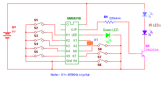
Circuit diagram tab 1 shows schematic diagram of transmitter circuit using chip SM5021B. Its 16 pin IC 8 pins are for 8 channels, 2 for power supply (Vcc (16) & Gnd (8)), 2 for crystal connections (X1(12) & X2(13)), 2 for custom code (C1 (1) & C2 (2)) and last 2 for output. One is for modulated output (o/p (15)) and other is for LED output (14).
Tx: Connection and Operation
Connections: – All key inputs of chip from K1 to K8 are connected to ground through push buttons switches S1 to S8. A 455 KHz crystal is connected between pins X1 & X2. Custom code pins C1 and C2 are directly connected to ground to setup a custom code 00. LED is directly connected to LED output pin. The modulated o/p pin drives two IR LEDs through transistor 2N2222A. 9V standard battery is connected to power supply pins.
Operation: – Whenever you press any switch that key i/p of IC is grounded and so a particular code is generated and transmitted. Every code is of 13 bits. The format of code is as given below
1 1 0 C1 C2 D7 D6 D5 D4 D3 D2 D1 D0
Start bits Custom code data bits
· First three bits are called start bits and they are always 110
· Next two bits are custom code set by user. You can set any of these combination 00,01,10 or 11 (I have set it 00 by connecting C1 & C2 to ground)
· Last 8 bits are data bits. The combination of these bits is different for each key input. Please refer the table given below
|
Start bits |
Custom Code |
D7 |
D6 |
D5 |
D4 |
D3 |
D2 |
D1 |
D0 |
Key input |
|||
|
1 |
1 |
0 |
C1 |
C2 |
0 |
0 |
0 |
0 |
0 |
0 |
0 |
1 |
K1 |
|
1 |
1 |
0 |
C1 |
C2 |
0 |
0 |
0 |
0 |
0 |
0 |
1 |
0 |
K2 |
|
1 |
1 |
0 |
C1 |
C2 |
0 |
0 |
0 |
0 |
0 |
1 |
0 |
0 |
K3 |
|
1 |
1 |
0 |
C1 |
C2 |
0 |
0 |
0 |
0 |
1 |
0 |
0 |
0 |
K4 |
|
1 |
1 |
0 |
C1 |
C2 |
0 |
0 |
0 |
1 |
0 |
0 |
0 |
0 |
K5 |
|
1 |
1 |
0 |
C1 |
C2 |
0 |
0 |
1 |
0 |
0 |
0 |
0 |
0 |
K6 |
|
1 |
1 |
0 |
C1 |
C2 |
0 |
1 |
0 |
0 |
0 |
0 |
1 |
1 |
K7 |
|
1 |
1 |
0 |
C1 |
C2 |
1 |
0 |
0 |
0 |
0 |
0 |
1 |
1 |
K8 |
These 13 bit codes are transmitted serially through modulated output pin o/p (15). IR LED will generate IR light beam of 38 KHz. At the same time green LED connected at LED output pin (14) will blink and indicate the code is transmitted.
Receiver
Receiver
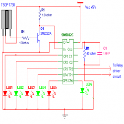
Circuit diagram tab 2 shows Receiver circuit using decoder IC SM5032C. It is 14 pin IC. 1 input pin (2), 1 oscillator pin (13), 2 for custom code (C1 (12) & C2 (13)), 2 for supply (Vcc (14), Gnd (1)) and rest 8 are 8 outputs. Out of these 8, 6 (CP1 to CP6) are pulse output and 2 (TP1 and TP2) are toggle output.
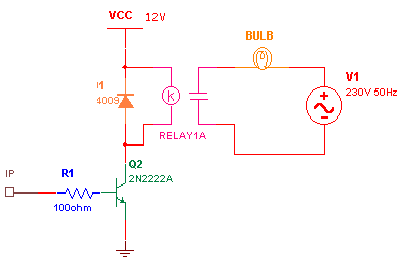
· Connection: – Output of IR sensor TSOP 1738 is connected to input of chip through transistor 2N2222A. Custom code pins C1 & C2 are directly connected to ground. Resistor R1 (43K?) and capacitor C1 (1nF) is connected to oscillator pin (13) as shown. LED is connected to each pulse output CP1 to CP6 and toggle outputs are connected to relay driving circuit. A typical relay firing circuit is as shown in figure below.

Fig. 1: Image showing a Typical Relay Firing Circuit
Operation: – IR sensor will detect 38 KHz IR light and recover the modulated code and give it to decoder chip. Decoder chip will compare start bits and custom code and if it matches then activates particular output depending upon the code received. Please refer the table.
|
Start bits |
Custom Code |
D7 |
D6 |
D5 |
D4 |
D3 |
D2 |
D1 |
D0 |
Output |
|||
|
1 |
1 |
0 |
C1 |
C2 |
0 |
0 |
0 |
0 |
0 |
0 |
0 |
1 |
CP1 |
|
1 |
1 |
0 |
C1 |
C2 |
0 |
0 |
0 |
0 |
0 |
0 |
1 |
0 |
CP2 |
|
1 |
1 |
0 |
C1 |
C2 |
0 |
0 |
0 |
0 |
0 |
1 |
0 |
0 |
CP3 |
|
1 |
1 |
0 |
C1 |
C2 |
0 |
0 |
0 |
0 |
1 |
0 |
0 |
0 |
CP4 |
|
1 |
1 |
0 |
C1 |
C2 |
0 |
0 |
0 |
1 |
0 |
0 |
0 |
0 |
CP5 |
|
1 |
1 |
0 |
C1 |
C2 |
0 |
0 |
1 |
0 |
0 |
0 |
0 |
0 |
CP6 |
|
1 |
1 |
0 |
C1 |
C2 |
0 |
1 |
0 |
0 |
0 |
0 |
1 |
1 |
TP1 |
|
1 |
1 |
0 |
C1 |
C2 |
1 |
0 |
0 |
0 |
0 |
0 |
1 |
1 |
TP2 |
So whenever you press switch S1 from transmitter LED1 will blink and if you press S2 LED2 will blink and so on. When you press S7 or S8 the toggle output TP1 and TP2 will be activated. So when you first press S7 or S8 TP1/TP2 will be high again when you press S7/S8 TP1/TP2 will be low. Thus TP1 and TP2 will energize or de-energize the relay on alternate key press. So you can get ON/OFF control for any AC/DC device.
Circuit Diagrams
Filed Under: Electronic Projects


Questions related to this article?
👉Ask and discuss on Electro-Tech-Online.com and EDAboard.com forums.
Tell Us What You Think!!
You must be logged in to post a comment.