Preparation of microcircuit lines utilizing a selective coating method. Just a hydrophilic region prepared through irradiation of parallel vacuum ultraviolet or PVUV is layered with metal ink. Also, an electrical circuit with a range width of 5um, created through the selective coating and electrode lines with distinct widths, lines as sleek as 1um can be prepared.
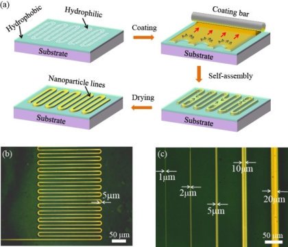
Figure 1: Electronic circuits printed at one micron resolution
A scientist panel comprising of MANA Independent Scientist Takeo Minari, International Centre for Materials Nanoarchitectonics (MANA), NIMS, and Colloidal Ink introduced a printing method for creating electrical circuits and sleek-layer transistors (TFTs) with line width and line spacing equal to 1um.
Printed electrical – printing techniques to structure electronic gadgets utilizing functional substances dissolved in ink – is withdrawing much focus in present years as a lucrative novel technique to form big-area semiconductor gadgets at a low price. Because such techniques allow the preparation of electrical gadgets even of flexible substrates, they are projected to be applicable to novel fields like wearable gadgets.
As compared to this, traditional printing technologies enable the creation of devices and circuits with line widths only as sleek as numerous dozen micrometres. Accordingly, they are not suitable to the formation of tiny gadgets ideal for practical use. Hence, there were great expectations for introducing novel printing methods potential of regularly fabricating circuits with line widths of multiple micro-metres or less.
In this experiment, the scientist group introducing a printing method potential of creating metal circuits with the line width being 1um on substrates that are flexible in nature. Utilizing such methods, they structured small organic TFTs. The aim of this printing method is as mainly to create hydrophilic and hydrophobic micro-patterns on the substrate by stimulating with parallel vacuum ultraviolet (PVUV) at a wavelength of 200 nanometres or less.
Then, a layer only the hydrophilic patterns with metal nanoparticle inks. The utilization of a PVUV light source allowed us to emphasis emitted light on much tinier targets than traditional light sources. In addition to this, the utilization of DryCure-Au-metal based nanoparticle ink that can create a conductive layer at room temperature introduced by Colloidal Ink – allowed us to create gadgets and circuits at room temperature during the complete process.
Conclusion – As a result, the experts were able to prevent distortion of substrates that become flexible by heat, and create and laminate circuits within the precision of multiple microns. Moreover, we accurately tuned the entrance overlap dimensions of the printed organic TFTs structured by this method, which was conventionally impossible due to precision issues. As a result, a practical moment level of 0.3 cm2 V-1 s-1 was achieved for the organic TFTs with the routing length of 1um. In upcoming experiments, we will plan to use the method in numerous fields like big-area flexible sensors and displays.
Filed Under: News

Questions related to this article?
👉Ask and discuss on EDAboard.com and Electro-Tech-Online.com forums.
Tell Us What You Think!!
You must be logged in to post a comment.