Controlling speed of AC motor is required in industries as well as in domestic use. In industries the required motion control is achieved by controlling speed of big and heavy AC motors. They use variable frequency drives (VFD) for speed control. In some other applications like fan, blowers, heaters etc another method for speed control is used that is phase angle control. By varying phase angle, the current supplied to motor can be varied. And by varying supplied current the speed of motor can be varied.
In domestic application the phase angle control method is used. The best example is fan regulator. In domestic fan regulator DIAC and TRIAC are used to vary phase angle of fan motor. This is very easiest method to vary AC motor speed.
Also the same principle can be applied to any heating element like heater. By changing the phase angle of AC waveform applied to heater the supplied current can be changed. And this will vary its temperature.
So in this project I am using this same principle to vary the speed of any 1 phase AC motor by varying phase angle of applied AC waveform. The phase angle is varied using DIAC and TRIAC only but DIAC and TRIAC are triggered by digital means using 8051 microcontroller. The speed variation is displayed on LED bar graph display. And the most interesting thing is the speed variation and motor ON / OFF control is done through RF remote control that has range of more than 100 meter.
System Block Diagram:

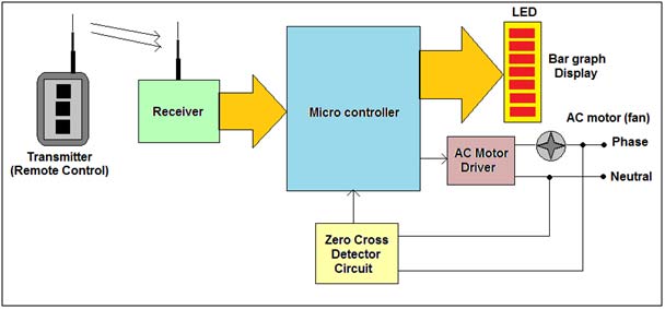
Fig. 1: Overview of RF Remote based AC Motor Controller
The figure shows building blocks of entire system. I am explaining each block one by one in brief.
Remote control (Transmitter): It is used to ON / OFF motor or to vary the speed of motor from remote place. Because its RF type (ASK) remote control, its range is around 150 meter. It sends particular codes for different keys over 434 MHz carrier frequency.
Receiver: It detects 434 MHz carrier and receives these key codes by demodulating it. Then it decodes the code and gives corresponding digital output to micro controller
Zero cross detector circuit: It generates short duration positive and negative pulses after every 10 ms (100 Hz) whenever applied 50 Hz AC signal crosses zero line. These pulses are given to micro controller
Micro controller: It controls speed of motor and also turns it ON or OFF. It also indicates motor speed on LED bar graph display. To vary the speed it varies the firing angle of thyristor. To vary firing angle it takes reference pulses from ZCD circuit.
AC Motor Driver: It gets firing pulses from micro controller and varies supplied current to motor by varying phase angle of thyristor.
LED Bar Graph: It indicates current motor speed on 8 LEDs. Maximum speed means all 8 LEDs are ON and minimum speed means single LED (lowest one) is ON.
Circuit description:
Complete circuit can be divided in following parts
1. Remote control circuit
2. Receiver circuit
3. Zero cross detector circuit
4. Micro controller circuit
Remote Control Circuit
Remote control circuit:

Fig. 2: Circuit Diagram of HT12E based RF Remote Control
Connections:- all the address lines A0-A7 are connected to ground (You can either connect all the lines to Vcc or to ground but keep in mind that on the receiver side you have to do same). This is to set same address both the sides. Resistor R1(1.1M?) is connected between oscillator pins (Osc1 & Osc2) to set transmitter frequency = 50×Receiver Frequency. Data lines D0-D3 are connected with switches S1-S3 through diodes D2-D4 respectively. The other terminal of all the switches is connected to ground. The TE pin (transmission enable) is also connected to all the switches through diodes D5-D7. The Dout pin of HT12E is connected to Din pin of 433.92MHz serial data transmitter. 9V standard battery supplies power to the circuit. A RED LED with current limiting resistor R2 is connected to TE pin to indicate data is transmitted.
Operation:-
Three push buttons are given for following operations
|
Button 1 |
ON / OFF motor |
|
Button 2 |
Increase motor speed |
|
Button 3 |
Decrease motor speed |
· Whenever any button is pressed particular data line is grounded and TE pin will be also grounded through another diode.
· So we can set the data at the same time we can pull the TE pin low by pressing single key
· When TE pin is low the address and data are transmitted serially through Dout pin.
· So 8-bit address and 4-bit data are together transmitted over 433.92MHz carrier frequency.
Receiver Circuit
Receiver Circuit:

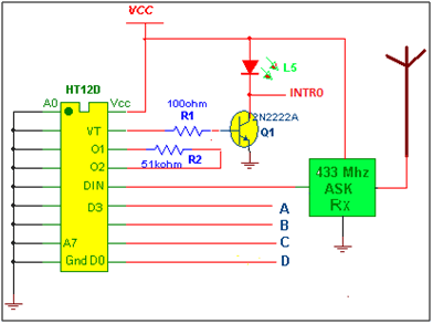
Fig. 3: Circuit Diagram of HT12D based RF Remote Receiver
Connections: All the address lines are connected to ground to set same address. Resistor R2 (51 K?) is connected between Oscillator pins. The Dout pin of 433.92 MHz serial data receiver is connected with Din pin of IC HT12D. RED LED L5 is connected to VT (valid transmission) pin through transistor Q1 to indicate valid transmission. All the data lines D0-D3 are connected to micro controller to give digital output corresponding to key press on transmitter.
Operation:
- When button is pressed from remote control, address & data are transmitted together
- The 433.92MHz serial data receiver will demodulate the carrier and gives this address & data to IC HT12D
- IC HT12D first compares the address three times and if it matches it gives high pulse on VT pin and latches the digital data on D0 – D4 that is given to micro controller.
- The high pulse on VT will generate short duration negative pulse on INT0 and LED L5 will blink. This INT0 pin generates external interrupt in micro controller
For example:
- Button 1 is pressed momentarily. So the data formed will be 1110 and address will be of course 00000000. Both are transmitted serially through ASK transmitter
- ASK receiver receives it, demodulated it and gives them to HT12D. HT12D first compares address thrice and if matches, gives high pulse on pin VT and then latch the same digital data 1110.
- LED blinks and external interrupt is generated for micro controller.
Zero Cross Detector Circuit
Zero cross detector circuit:

Fig. 4: Circuit Diagram of Zero Cross Detector
Connections: as shown in above figure transformer T1 step downs 230 VAC in to 9 VAC and this is given to bridge rectifier D1. This rectified output is fed to base of Q1 through diode D3 and voltage divider formed by resistors R1 & R2. Same rectified output is filtered through C1 and given to voltage regulator IC 7805. Output of 7805 is regulated 5 VDC that is given as biasing voltage for both transistors Q1 & Q2 (same regulated 5 V supply is given to main control section also). Both transistors are connected in switch configuration. The final output ‘C’ is given as external interrupt INT1 to micro controller.
Operation:- complete operation can be well understood with the help of wave forms.

Fig. 5: Diagram of Zero Cross Detection on Rectified AC Waveform
- As shown in figure the first wave form is full rectified wave that is fed to the base of Q1. Whenever this voltage falls below 0.7 V Q1 is switched off. So its output goes high.
- This will produce one very short positive pulse at ‘B’ as shown in figure as second waveform
- As this positive pulses are fed to Q2 which is again connected in switch configuration, it will produce one negative pulse at INT1 of same width of positive pulse. This is shown as third waveform
- These pulses are used to generate external interrupt in micro controller
Microcontroller Circuit
Micro controller circuit:
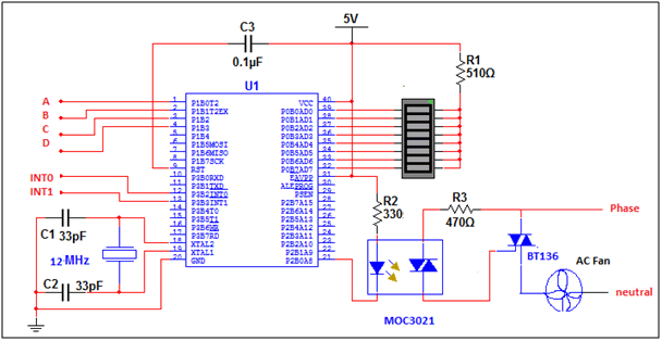
[As shown in the Circuit Diagram tab]Connections: four digital outputs of receiver circuit are connected to port P1 pins P1.0 to P1.3. The output of ZCD circuit INT0 is connected to external interrupt 0 pin P3.2 and INT1 output of receiver circuit is connected to external interrupt 1 pin P3.3. A 8 LED bar graph is connected to port P0. All the cathode terminals are connected to port pins and common anode terminal is connected to 5 V supply through current limiting resistor R1. The port P2 pin P2.0 is connected to cathode input of LED in opto coupler chip MOC3021. The diac of MOC3021 is connected to gate input of triac BT136. An AC fan (motor) is connected between AC supply with triac in between as shown. A 12 MHz crystal is connected to crystal input pins of microcontroller. Two 33 pF capacitors are connected with crystal to provide stability and biasing.
Operation:
· Initially motor is stop. All LEDs of bar graph are off. Micro controller is getting continuous pulses from ZCD circuit on INT1 pin.
· When start / stop button is pressed on remote control, micro controller gets INT0 from receiver circuit and it takes digital input from it on P1
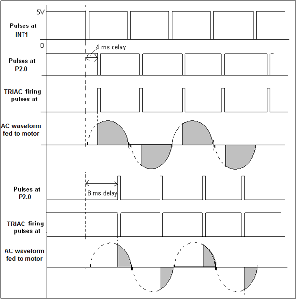
· Now onwards every time when it gets pulse on INT1 from ZCD, it will generate negative pulse on P2.0 after specified delay
· This negative pulse will turn on internal diac. The diac gives gate pulse to triac. The triac turns ON and this makes AC motor ON
· The speed of AC motor depends upon the delay between INT1 pulse and the pulse given to P2.0
· If delay is more the triac is fired later so less current supplied to motor and motor speed is less
· If delay is less, the triac is fired earlier that means more current supplied to motor and motor speed is more
· The delay is increased or decreased by pressing buttons 3 and 2 respectively on remote control
· If button 2 is pressed while motor is running, the delay is decreased and motor speed is increased. The LED bar graph grows up by one step (LED)
· If button 3 is pressed while motor is running, the delay is increased and motor speed is decreased. The LED bar graph falls down by one step (LED)
· If button 1 is pressed again the micro controller will stop sending pulses to MOC3021 that will stop motor. To start motor again press same button.
· The waveforms given in figure gives more better idea

Fig. 6: Diagram of Output Waveforms from TRIAC to AC Motor
Project Source Code
###
/* The software program for 89C51 micro controller is written in C language. It is compiled, simulated, debugged in KEIL (IDE). Here is complete C program code with comments. */ #include<reg51.h> sbit op = P2^0; unsigned int i=0,c=0,d=8; unsigned char byte[9]={0xFF,0x7F,0x3F,0x1F,0x0F,0x07,0x03,0x01,0x00}; unsigned char byt; void keydly() // key debounce delay { int p,q; for(p=0;p<30;p++) for(q=0;q<1000;q++); } void delay(int d) // basic 1 ms delay subroutine { int r; TL0 = 0x26; TH0 = 0xFC; TR0 = 1; for(r=0;r<d;r++) { while(TF0==0); TF0 = 0; TL0 = 0x26; TH0 = 0xFC; } TR0 = 0; } void int0(void) interrupt 0 // external interrupt 1 subroutine { byt=P1; // get digital input on P1 } void int1(void) interrupt 2 // external interrupt 2 subroutine { int t; if(d!=0) delay(d); // apply output pulse after delay else for(t=0;t<50;t++); op=0; for(t=0;t<100;t++); op=1; } void main() { TMOD = 0x01; // initialize timer0 as 16 bit timer P1=0xFF; // P1 as input port op=0; // P2.0 as output op=1; P0=0x00; // P0 as output port P0=byte[i]; // motor off LED off IE=0x81; // enable external interrupt 0 only IT0=1; IT1=1; back: byt=0xFF; while(byt==0xFF); //loop until no key is pressed keydly(); // key debounce delay switch(byt) { case 0xF7: // for button 3 if(d>0) d--; // decrease delay if(i<9) i++; // increase bar graph P0=byte[i]; break; case 0xFB: // for button 2 if(d<8) d++; // increase delay if(i>0) i--; P0=byte[i]; // decrease bar graph break; case 0xFD: // for button 1 c++; // enable or disable ext int 1 if((c%2)==1) {EX1=1; P0=byte[i];} else {EX1=0; P0=byte[0];} break; } goto back; // continuous loop }###
Circuit Diagrams
Project Video
Filed Under: Electronic Projects
Filed Under: Electronic Projects


Questions related to this article?
👉Ask and discuss on Electro-Tech-Online.com and EDAboard.com forums.
Tell Us What You Think!!
You must be logged in to post a comment.