IESA seeks chips for various products such as smartcards, energy meters, LED lighting, rural broadband, and IoT incorporations in various sectors. The new accelerator is also looking to build a local station of semiconductor startups that can devise chips for India-specific necessities. The aim is to incubate three or four startups in 2019.
India is lagging compared to most global semiconductor manufacturing companies. However, the country has the potential to build several semiconductor design firms, similar to Intel, Cadence, and Texas Instruments (which all have software development bases in India).
The country’s new Semiconductor Fabless Accelerator Lab (SFAL) — a first-of-its-kind center for research and excellence in the semiconductor industry — will provide the infrastructure to build intellectual property in the area of semiconductors. To date, the Karnataka government has invested Rs 21.5 crore in the accelerator, which is expected to rise to Rs 56 crores in five years.
Essentially, SFAL will fill the gap in the electronic system design and manufacturing (ESDM) ecosystem, providing India with the chance to capitalize on intelligent electronics. According to the IESA report at Vision Summit 2018, the Indian semiconductor component market is forecasted to see a significant market increase of USD 32.35 Bn by 2025.
Startup challenges
Many startups are struggling to succeed in the semiconductor sector because of costs. Aside from the initial business investment, startups require considerable industry knowledge and favorable government policies. The government’s Make in India initiative — with the aim of job creation and skill enhancement in 25 sectors of the economy — is one program supporting the semiconductor sector.
However, a lack of funding remains one of the biggest roadblocks for most startups. Better client connections and market access are other challenges.
So far, manufacturing has been the focus from a political standpoint. The United Progressive Alliance (UPA) and National Democratic Alliance (NDA) governments have made promises to set up semiconductor fabrication plants, which manufacture integrated circuits. However, only two fabrication plans have been constituted — one in Chandigarh by ISRO and another in Gujarat.
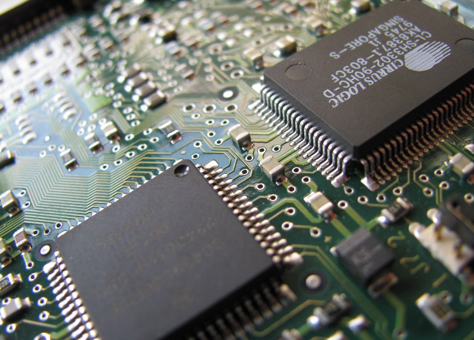
Interestingly, India imports about 90 percent of its electronics components. Although the government has expressed concerns about this figure, little has been done to change it. Semiconductor start-ups in India are, therefore, competing against multi-national organizations. This is where IESA can make a difference.
IESA comptrollers announced that a contingent of 12 senior industry managers are delivering “on-ground activation” for securing startup innovation and investment.
Funding & market access
Startups are currently shelling out about USD 20,000 for hardware and software, spending six years minimum building and marketing a prototype, and paying employees. After the product launch, alterations may still be required and market access can take significant time.
Additionally, many in the semiconductor sector are concerned about the goal of some venture capitalists (VCs), which seem misaligned with the manufacturing ones of the government. For example, startups are questioning the focus of certain VCs. Some are investing USD 10 to 15M in e-commerce or food-tech ventures, which are proving unsuccessful (and fail to relate to manufacturing). However, few are investing comparable funds in the semiconductor sector, which seems far more promising.
China, for example, has been accounted for 44 percent of the global semiconductor industry’s total revenue of USD 339 Bn, according to the Semiconductor Industry Association.
What’s more is that as connected devices become more mainstream, the government faces an increased security risk. Therefore, semiconductor funding is particularly significant. Fortunately, the Karnataka government’s new accelerator facility has sanctioned for 200 start-ups, and the government has offered extensive support, funding, and market access.
Revolutionary semiconductor R&D
Here’s one example of the benefit of investing in the semiconductor sector: Two ultra-thin materials with different properties were placed one on top of the other, providing a new, useful element with hybrid characteristics.
This approach was taken by an international community of researchers, with brace atomic-level semiconductor elements, which resulted in elements that are hybrid and further tunable. The characteristics are crystalline layers of atoms, comprising one-millionth of a human hair in density. Scientists describe such atomic elements two-dimensional (2D).
These two atomic layers are appended solely by a force identified as “van der Waals interaction,” or a distance-dependent interaction between atoms or molecules. The substances used in the research are monolayers of tungsten disulfide and molybdenum diselenide. The new element has semiconducting properties similar to that of silicon-based components used in diminutive electronics.
This revolutionary material could be the silicon of the expectation since it is semiconducting, as well as manageable, lightweight, adjustable and stretchable. Silicon-based corporealities are three dimensional (3D).
Filed Under: Blog entry, Tech Articles

Questions related to this article?
👉Ask and discuss on Electro-Tech-Online.com and EDAboard.com forums.
Tell Us What You Think!!
You must be logged in to post a comment.