[[wysiwyg_imageupload:1622:]]
This Project is done by Mr. Arun Kumar.
In this fast moving world, new technologies have been evolved for every second for our human life style improvement. There have enormous advancement in automobile technologies already and still to come. Because of these technologies, now we are enjoying the necessary comfort and safety.
INTRODUCTION
1.2 MQ303A Alcohol Sensor
 Characteristics
Alcohol Sensor Circuit
• Detection Range: 100 – 10,000 ppm iso-butane propane
• Fast Response Time: <10s
• Heater Voltage: 5.0V
• Dimensions: 18mm Diameter, 17mm High excluding pins, Pins – 6mm High
Normal
0
false
false
false
EN-US
X-NONE
X-NONE
/* Style Definitions */
table.MsoNormalTable
{mso-style-name:”Table Normal”;
mso-tstyle-rowband-size:0;
mso-tstyle-colband-size:0;
mso-style-noshow:yes;
mso-style-priority:99;
mso-style-qformat:yes;
mso-style-parent:””;
mso-padding-alt:0in 5.4pt 0in 5.4pt;
mso-para-margin:0in;
mso-para-margin-bottom:.0001pt;
mso-pagination:widow-orphan;
font-size:10.0pt;
font-family:”Calibri”,”sans-serif”;}
1.3 INTERFACING THE CONTROL CIRCUIT TO THE IGNITION SYSTEM
The battery supplies large power to the spark plug so direct interfacing of the logic circuit will burn the IC’s. so relay switches are used. The battery circuit consist of a NC relay switch. The NC switch is controlled by a solenoid which is energized by the signals from the logic circuit. The power for energizing the coils is obtained by amplifying the IC signals using a transistor.
The microprocessor is programmed with a time program for a duration of ten seconds such that at the end of the program the microprocessor automatically opens the ignition circuit. Now when the logic circuit gives output as logic 1 the micro processor’s program is brought to a end without any result so the NC is left undisturbed. When no signal is obtained from the logic circuit that’s logic zero, the processor’s program runs fully and at the end of the program the solenoid of the NC is energized which pulls the NC switch off the circuit so the circuit is opened. Due to this the engine will not crank.

In this case a solenoid actuated needle is inserted into the spring nozzle which is controlled by the signal from the micro processor. So when logic 0 is detected the needle will be fully inserted and no fuel spray takes place else normal operation is carried out.
1.3 SEQUENCE OF OPERATION FOR ALCOHOL DETECTION SYSTEM WHILE STARTING
1. The driver puts the ignition key and gives the first step turn. This closes the electrical circuit of the car.
2. The solenoid port opens and the mask is dropped down, at the same time the salt inlet port of alcohol testing chamber is opened and exit port is closed.
3. Air reaches the testing chamber and detection process is carried out.
4. Depending upon the output the engine is cranked
1.4 DETECTION OF ALCOHOL DURING DRIVING
The fact used in this process is that on consumption of alcohol the pulse rate decreases. But the pulse rate varies significantly for different persons. So after initial testing the pulse rate of the person is recorded using pulse sensors. The pulse sensors consist of very sensitive miniature piezo film which gets deflected by the blood pulses. The number of pulses per minute is recorded by a counter circuit. The initial reading is taken as reference and periodic checks are made by the sensors, if there is significant reduction is pulse rate then the car stops.
Thus a design to efficiently check drunken driving has been developed. By implementing this design a safe car journey is possible decreasing the accident rate due to drinking. By implementing this design drunken drivers can be controlled so are the accidents due to drunken driving. Government must enforce laws to install such circuit is every car which are already on road and must regulate all car companies to preinstall such mechanisms while manufacturing the car itself. If this is achieved the deaths due to drunken drivers can be brought to zero percent.
2. CAR THEFT: INTRODUCTION
As India is emerging as an economic power country, many people are now being able to afford cars. This shows the power of the country but like double-edged sword this development in other hand, has given rise to a most jeopardizing crime that is cars theft. There has been a gradual increasing in the incidence of cars lifting. These stolen cars are then again sold out by changing their chassis number in another city or neighboring countries. Thieves also find it profitable to sell expensive equipment and accessories of the car such as batteries, stereos and other decorative tools of the cars. Ministers also confessed that, car-lifting cases have shown an increasing trend, but there is a declining trend in tracing of these vehicles. Without any method of tracking the cars, only 10 percent of the total stolen vehicles are recovered.
CAR THEFT DATA IN INDIA
According to official sources of Ministry of State for Home Affairs, the rate of car hacking is increasing year by year. In the year 2003, the total 68,945 cases of car theft were registered, while it becomes 80,750 cases in 2004. In 2005 and 2006, total number of cases came in the limelight were 84,150 and 83,375 respectively, in which the exact figure of total cases of the year is still awaiting, because the above figure of the data is till Sep 2006. That’s why the government is extremely worried about the vehicle theft crime and appeals to the owners to utilize the advance techniques of the GPS and others related techniques available in the market to reduce the car theft cases. These cases harms the country and the society worth millions and millions dollars.
2.1 WHAT IS GPS TRACKING DEVICE?
GPS is a compact handy device like mobile phone with enabled combo technology of GPS and GPRS that track mobile vehicles through using four visible satellites. The satellites send the signals to the GPS receiver and it calculates the signals and inform about the exact position of the vehicle on the earth. The calculated data send on web server provided to users by the GPS service providing company. The company provides a web based login account to access the data from the web server. Using this account, the user can track one or more vehicles at a time. The GPS Device provides the complete data about your vehicle like its status, maximum speed, motion hours, distance covered and stationary timing and duration.
2.2 MICRO VEHICLE BLACK BOX
Micro vehicle black box is a next generation anti-theft security system. This is a new concept, which is in a testing phase to track the stolen car through cell phones. It is compatible with all GSM or CDMA mobiles. With the help of this service, it will be easy to make the car immobilize, also this service will help to know about the unauthorized entry in the car, and location of the vehicle. Through this service it will be easy to make two-way communication with the driver and transfer of command.
2.3 WORKING OF ANTI-THEFT SYSTEM
This concept implements a low cost object tracking system using GPS and GPRS. The system allows a user to view the present and the past positions recorded of a target object on Google Map through the internet. The system reads the current position of the object using GPS, the data is sent via GPRS service from the GSM network towards a web server using the POST method of the HTTP protocol.
The object’s position data is then stored in the database for live and past tracking. A web application is developed using PHP, JavaScript, Ajax and MySQL with the Google Map embedded. The existing live tracking systems that are available now a days use SMS for the communication to the server which turned out to be expensive. (SMS are used for communication to device). We have used the GPRS service which made our system a low cost tracking solution for localizing an object position and status. This system is very useful for car theft situations (alarm alert, engine starting, localizing), for adolescent drivers being watched and monitored by parents (speed limit exceeding, leaving a specific area), as well as for human and pet tracking.
A good number of tracking systems had so far been developed with a wide range of tracking facilities. But the operation cost of most of these systems is higher which prevents from widespread use. On the other hand, the rate of car theft, asset theft, child kidnapping in many countries are increasing at a higher rate. The objective of this research is to reduce the cost of the tracking system using the latest technologies and making it available to the common people.
2.4. HARDWARE SPECIFICATION
We need a module which is compatible with 850MHZ/900MHz/1800MHz/190OMhz frequencies of cellular networks. Telit GM862-GPS GPS/GPRS is the module we have selected for this system shown in Fig 2. This device is capable of working in any GSM network around the world.
It has a python interpreter with 3MB Non-volatile memory and a 1.5 MB volatile memory integrated inside the module [9]. No external controller is required. It has a 20 channel high sensitive GPS receiver and built-in SIM card holder. This makes the system compact and power efficient. To build a complete working system using this module, only the power source and the antenna is required. It also supports complete standard AT command set plus custom AT command set for GPS. Sent to the server as a string. Then after a certain time period it checks the availability of GPRS and connects to the HTTP server. The current location of the device is sent. In this way the device communicates with the server and sends the location.
2.7. DISCUSSION ON LOW COST SOLUTION
Efforts have been taken to reduce the total cost of the system including device and services. The device cost is reduced by using a single module solution. By using free Google map API and HTTP protocol the service cost has been reduced dramatically. Starting from small business to large enterprise, the device and service cost can be affordable. They can also set up their own customized web-based remote monitoring system easily. To reduce the total system cost, a single GSM/GPRS/GPS module was used instead of separate devices. It requires only external power and an antenna for GPS and GSM. Beside the cost, this approach saves extra PCB space of the system. On the other hand, it is integrated with high level python language interpreter. This makes it easy to program, update and optimize the system and additionally save the external controller. Moreover, it saves development time and cost compared to programming and interfacing external controller.

Using mobiles while driving is one of vital cause for accidents. Even though the rules are enhanced, most of the people not obeying it. In our concept, we provided the kit which supports the rule and save our human life. The mobile sniffing system is shown below.
During travelling, if he uses mobile phones then he/she is allowed to use not more than 15 seconds. Then a voice message about stop using mobiles will be given. If still he/she continues, the vehicle will get slow and stops.

BLOCK DIAGRAM:-
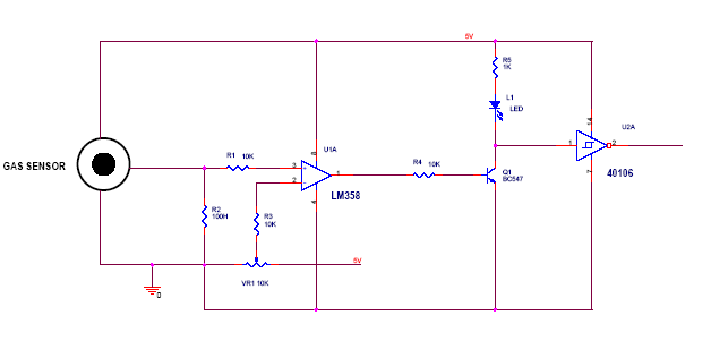
ALCOHOL SENSOR
Ideal sensor for use to detect the presence of a dangerous alcohol use and drive or in a service station, storage tank environment. This unit can be easily incorporated into an alarm unit, to sound an alarm or give a visual indication of the LPG concentration. The sensor has excellent sensitivity combined with a quick response time.
The gas sensor is the special sensor which designed for sense the gas leakage. In the gas sensor the supply voltage is given to input terminal. The gas sensor output terminals are connected to non inverting input terminal of the comparator.
Here the comparator is constructed with operational amplifier LM 358. When there is no leakage the non inverting input is grater then inverting input so the output of the comparator is positive voltage which is given to the base of the switching transistor BC 547.
Hence the transistor is conducting. Here the transistor is act as switch so the collector and emitter will be closed. The output is taken from collector terminal. Now the output is zero which is given to hex inverter 40106.
When there is gas leakage the inverting input voltage is grater than non inverting input. Now the comparator output is -12V so the transistor is cutoff region. The 5v is given to hex inverter 40106 IC. Then the final output data is directly given to microcontroller to determine the gas leakage.
Relay
RELAY
A relay is an electrically operated switch. Current flowing through the coil of the relay creates a magnetic field which attracts a lever and changes the switch contacts. The coil current can be on or off so relays have two switch positions and they are double throw (changeover) switches. Relays allow one circuit to switch a second circuit which can be completely separate from the first. For example a low voltage battery circuit can use a relay to switch a 230V AC mains circuit. There is no electrical connection inside the relay between the two circuits; the link is magnetic and mechanical.
The coil of a relay passes a relatively large current, typically 30mA for a 12V relay, but it can be as much as 100mA for relays designed to operate from lower voltages. Most ICs (chips) cannot provide this current and a transistor is usually used to amplify the small IC current to the larger value required for the relay coil. The maximum output current for the popular 555 timer IC is 200mA so these devices can supply relay coils directly without amplification. 

Relays are usually SPDT or DPDT but they can have many more sets of switch contacts, for example relays with 4 sets of changeover contacts are readily available. Most relays are designed for PCB mounting but you can solder wires directly to the pins providing you take care to avoid melting the plastic case of the relay. The animated picture shows a working relay with its coil and switch contacts.
You can see a lever on the left being attracted by magnetism when the coil is switched on. This lever moves the switch contacts. There is one set of contacts (SPDT) in the foreground and another behind them, making the relay DPDT.

The relay’s switch connections are usually labeled COM, NC and NO:
- COM = Common, always connect to this, it is the moving part of the switch.
- NC = Normally Closed, COM is connected to this when the relay coil is off.
- NO = Normally Open, COM is connected to this when the relay coil is on.
Circuit description:
This circuit is designed to control the load. The load may be motor or any other load. The load is turned ON and OFF through relay. The relay ON and OFF is controlled by the pair of switching transistors (BC 547). The relay is connected in the Q2 transistor collector terminal. A Relay is nothing but electromagnetic switching device which consists of three pins. They are Common, Normally close (NC) and Normally open (NO).
The relay common pin is connected to supply voltage. The normally open (NO) pin connected to load. When high pulse signal is given to base of the Q1 transistors, the transistor is conducting and shorts the collector and emitter terminal and zero signals is given to base of the Q2 transistor. So the relay is turned OFF state.
When low pulse is given to base of transistor Q1 transistor, the transistor is turned OFF. Now 12v is given to base of Q2 transistor so the transistor is conducting and relay is turned ON. Hence the common terminal and NO terminal of relay are shorted. Now load gets the supply voltage through relay.
Voltage Signal from Transistor Q1 Transistor Q2 Relay
Microcontroller or PC
1 on off off
0 off on on
RS232 Communication
RS232 COMMUNICATION

RS232:
In telecommunications, RS-232 is a standard for serial binary data interconnection between a DTE (Data terminal equipment) and a DCE (Data Circuit-terminating Equipment). It is commonly used in computer serial ports.
Scope of the Standard:
The Electronic Industries Alliance (EIA) standard RS-232-C [3] as of 1969 defines:
- Electrical signal characteristics such as voltage levels, signaling rate, timing and slew-rate of signals, voltage withstand level, short-circuit behavior, maximum stray capacitance and cable length
- Interface mechanical characteristics, pluggable connectors and pin identification
- Functions of each circuit in the interface connector
- Standard subsets of interface circuits for selected telecom applications
The standard does not define such elements as character encoding (for example, ASCII, Baudot or EBCDIC), or the framing of characters in the data stream (bits per character, start/stop bits, parity). The standard does not define protocols for error detection or algorithms for data compression.
The standard does not define bit rates for transmission, although the standard says it is intended for bit rates lower than 20,000 bits per second. Many modern devices can exceed this speed (38,400 and 57,600 bit/s being common, and 115,200 and 230,400 bit/s making occasional appearances) while still using RS-232 compatible signal levels.

In this circuit the microcontroller transmitter pin is connected in the MAX232 T2IN pin which converts input 5v TTL/CMOS level to RS232 level. Then T2OUT pin is connected to reviver pin of 9 pin D type serial connector which is directly connected to PC.

Buzzer:
A buzzer or beeper is a signalling device, usually electronic, typically used in automobiles, household appliances such as a microwave oven, or game shows. It most commonly consists of a number of switches or sensors connected to a control unit that determines if and which button was pushed or a preset time has lapsed, and usually illuminates a light on the appropriate button or control panel, and sounds a warning in the form of a continuous or intermittent buzzing or beeping sound. Initially this device was based on an electromechanical system which was identical to an electric bell without the metal gong (which makes the ringing noise).
Often these units were anchored to a wall or ceiling and used the ceiling or wall as a sounding board. Another implementation with some AC-connected devices was to implement a circuit to make the AC current into a noise loud enough to drive a loudspeaker and hook this circuit up to a cheap 8-ohm speaker. Nowadays, it is more popular to use a ceramic-based piezoelectric sounder like a Sonalert which makes a high-pitched tone. Usually these were hooked up to “driver” circuits which varied the pitch of the sound or pulsed the sound on and off.
Circuit Description
Circuit Description:
The circuit is designed to control the buzzer. The buzzer ON and OFF is controlled by the pair of switching transistors (BC 547). The buzzer is connected in the Q2 transistor collector terminal.
When high pulse signal is given to base of the Q1 transistors, the transistor is conducting and close the collector and emitter terminal so zero signals is given to base of the Q2 transistor. Hence Q2 transistor and buzzer is turned OFF state.
When low pulse is given to base of transistor Q1 transistor, the transistor is turned OFF. Now 12v is given to base of Q2 transistor so the transistor is conducting and buzzer is energized and produces the sound signal.

The present chapter introduces the operation of power supply circuits built using filters, rectifiers, and then voltage regulators. Starting with an ac voltage, a steady dc voltage is obtained by rectifying the ac voltage, then filtering to a dc level, and finally, regulating to obtain a desired fixed dc voltage. The regulation is usually obtained from an IC voltage regulator unit, which takes a dc voltage and provides a somewhat lower dc voltage, which remains the same even if the input dc voltage varies, or the output load connected to the dc voltage changes.
A block diagram containing the parts of a typical power supply and the voltage at various points in the unit is shown in fig 19.1. The ac voltage, typically 120 V rms, is connected to a transformer, which steps that ac voltage down to the level for the desired dc output. A diode rectifier then provides a full-wave rectified voltage that is initially filtered by a simple capacitor filter to produce a dc voltage. This resulting dc voltage usually has some ripple or ac voltage variation. A regulator circuit can use this dc input to provide a dc voltage that not only has much less ripple voltage but also remains the same dc value even if the input dc voltage varies somewhat, or the load connected to the output dc voltage changes. This voltage regulation is usually obtained using one of a number of popular voltage regulator IC units.
IC VOLTAGE REGULATORS:
Voltage regulators comprise a class of widely used ICs. Regulator IC units contain the circuitry for reference source, comparator amplifier, control device, and overload protection all in a single IC. Although the internal construction of the IC is somewhat different from that described for discrete voltage regulator circuits, the external operation is much the same. IC units provide regulation of either a fixed positive voltage, a fixed negative voltage, or an adjustably set voltage.
A power supply can be built using a transformer connected to the ac supply line to step the ac voltage to desired amplitude, then rectifying that ac voltage, filtering with a capacitor and RC filter, if desired, and finally regulating the dc voltage using an IC regulator. The regulators can be selected for operation with load currents from hundreds of milli amperes to tens of amperes, corresponding to power ratings from milliwatts to tens of watts
THREE-TERMINAL VOLTAGE REGULATORS:
Fig shows the basic connection of a three-terminal voltage regulator IC to a load. The fixed voltage regulator has an unregulated dc input voltage, Vi, applied to one input terminal, a regulated output dc voltage, Vo, from a second terminal, with the third terminal connected to ground. For a selected regulator, IC device specifications list a voltage range over which the input voltage can vary to maintain a regulated output voltage over a range of load current. The specifications also list the amount of output voltage change resulting from a change in load current (load regulation) or in input voltage (line regulation).
SMCL – LCD
AT89CS1 is the 40 pins, 8 bit Microcontroller manufactured by Atmel group. It is the flash type reprogrammable memory. Advantage of this flash memory is we can erase the program within few minutes. It has 4kb on chip ROM and 128 bytes internal RAM and 32 I/O pin as arranged as port 0 to port 3 each has 8 bit bin .Port 0 contain 8 data line(D0-D7) as well as low order address line(AO-A7). Port ` contain higher order address line (A8-A15). Port 3 contains special purpose register such as serial input receiver register SBUF, interrupt INT0,INT1 and Timers T0 , T1 many of the pins have multi functions which can be used as general purpose I/P pins (or) Special purpose function can be decided by the programmer itself.
CRYSTAL
The heart of the micro controller is the circuitries which generate the clock pulse. Then micro controller provides the two pins. XTAL 1, XTAL 2 to correct the external crystal resonator along with capacitor. The crystal frequency is the basic clock frequency of the microcontroller.
RESET
The memory location for 89C51 0000H to 0FFFH. Whenever switch on the supply the memory location starts from 0000H.The 89C51 micro controller provide 9th pin for Reset Function.
Here the reset circuitry consists of 10Mf capacitor in series with 10K resister. When switch on the supply the capacitor is changed and discharged gives high low pulse to the 9th pin through the 7414 inverter.
Here we interface LCD display to microcontroller via port 0 and port 2. LCD control lines are connected in port 2 and Data lines are connected in port 0.
LCD
Liquid Crystal Display has 16 pins in which first three and 15th pins are used for power supply. 4th pin is RS (Register Selection) if it is low data and if it is high command will be displayed. 5th pin is R/W if it is low it performs write operation. 6th pin act as enable and remaining pins are data lines
Microcontroller
MICRO CONTROLLER
INTRODUCTION
Microcontrollers are destined to play an increasingly important role in revolutionizing various industries and influencing our day to day life more strongly than one can imagine. Since its emergence in the early 1980’s the microcontroller has been recognized as a general purpose building block for intelligent digital systems. It is finding using diverse area, starting from simple children’s toys to highly complex spacecraft. Because of its versatility and many advantages, the application domain has spread in all conceivable directions, making it ubiquitous. As a consequence, it has generate a great deal of interest and enthusiasm among students, teachers and practicing engineers, creating an acute education need for imparting the knowledge of microcontroller based system design and development. It identifies the vital features responsible for their tremendous impact, the acute educational need created by them and provides a glimpse of the major application area.
FEATURES
• Fully Static Operation: 0 Hz to 24 MHz
• Three-Level Program Memory Lock
• 128 x 8-Bit Internal RAM
• 32 Programmable I/O Lines
Port 0
Port 0 is an 8-bit open drain bidirectional I/O port. As an output port each pin can sink eight TTL inputs. When 1s are written to port 0 pins, the pins can be used as highimpedance inputs. Port 0 may also be configured to be the multiplexed loworder address/data bus during accesses to external program and data memory. In this mode P0 has internal pullups. Port 0 also receives the code bytes during Flash programming, and outputs the code bytes during program verification. External pullups are required during program verification.
Port 1
Port 1 is an 8-bit bidirectional I/O port with internal pullups. The Port 1 output buffers can source four TTL inputs. When 1s are written to Port 1 pins they are pulled high by the internal pullups and can be used as inputs. As inputs, Port 1 pins that are externally being pulled low will source current (IIL) because of the internal pullups. Port 1 also receives the low-order address bytes during Flash programming and verification.
Port 2
Port 2 is an 8-bit bidirectional I/O port with internal pullups. The Port 2 output buffers can /source four TTL inputs. When 1s are written to Port 2 pins they are pulled high by the internal pullups and can be used as inputs. As inputs, Port 2 pins that are externally being pulled low will source
Port 3
Port 3 is an 8-bit bidirectional I/O port with internal pullups. The Port 3 output buffers can sink/source four TTL inputs. When 1s are written to Port 3 pins they are pulled high by the internal pullups and can be used as inputs. As inputs, Port 3 pins that are externally being pulled low will source current (IIL) because of the pullups. Port 3 also serves the functions of various special features of the AT89C51 as listed below: Port 3 also receives some control signals for Flash programming and verification.
Port Pin Alternate Functions
P3.0 RXD (serial input port)
P3.1 TXD (serial output port)
P3.2 INT0 (external interrupt 0)
P3.3 INT1 (external interrupt 1)
P3.4 T0 (timer 0 external input)
P3.5 T1 (timer 1 external input)
P3.6 WR (external data memory write strobe)
P3.7 RD (external data memory read strobe)
RST
Reset input. A high on this pin for two machine cycles while the oscillator is running resets the device.
ALE/PROG
Address Latch Enable output pulse for latching the low byte of the address during accesses to external memory. This pin is also the program pulse input (PROG) during Flash programming. In normal operation ALE is emitted at a constant rate of 1/6 the oscillator frequency, and may be used for external timing or clocking purposes. Note, however, that one ALE pulse is skipped during each access to external Data Memory. If desired, ALE operation can be disabled by setting bit 0 of SFR location 8EH. With the bit set, ALE is active only during a MOVX or MOVC instruction. Otherwise, the pin is weakly pulled high. Setting the ALE-disable bit has no effect if the microcontroller is in external execution mode.
PSEN
Program Store Enable is the read strobe to external program memory.
MICROCONTROLLER AT89S52

9.1. PIN DIAGRAM
9.2. DESCRIPTION
The AT89S52 is a low power, high performance CMOS 8-bit microcomputer with 8k bytes of flash programmable and erasable read only memory (PEROM). The devices manufactured using Atmel’s high-density non-volatile memory technology and are compatible with the industry-standard 80S51 and X52 instruction set and pin out.
The on-chip flash allows the program memory to be reprogrammed in system or by a conventional non-volatile memory programmer. By combining a versatile 8-bit CPU flash on a monolithic chip, the Atmel AT89S52 is a powerful micro computer which provides a highly – flexible and cost-effective solution to many embedded control application.
9.3. PROGRAMMABLE PORTS:
PORT 0:
Port 0 is an 8-bit open drain bi-directional i/o port. As an output port, each tin can sink eight TTL inputs. When 1’s is written to port 0 pins, the pins can be used as high-impedance inputs. Port 0 can also be configured to be the multiplexed low-order address/data us during access to external program and data memory. In this mode port 0 as internal pull ups. Port 0 also receives the code bytes during rash programming and outputs the code bytes during program verification. External pull ups are required during program verification.
PORT 1:
Port 1 is an 8-bit bi–bit open drain bi-directional i/o port with internal pull ups. The port 1input buffers can sink/source four TTL inputs. When 1’s is written to port 1 pin they are pulled high by the internal pull ups and can be used as inputs. As inputs, port 1 pins that are externally being pulled low will source current because of the internal pull ups. In addition, P1.0 and P1.1 can be configured to be the timer/counter to external count inputs and the timer/counter to trigger input, respectively. Port 1 also receives low-order address bytes during flash programming and verification.
PORT 2:
Port 2 is an 8-bit bi–bit open drain bi-directional port with internal pull ups. The port 2 output buffer can sink/source four TTL inputs. When 1’s is written to port 2 pins they are pulled high by the internal pull ups and can be used as inputs. As inputs, port 2 pins that are externally being pulled low will source current because of the internal pull ups. Port 2 emits the high-order address byte during from external program memory and during accesses to external data memory that uses 16-bit addresses (MOV X @ DPTR). In this application, port 2 uses strong pull ups when emitting 1’s during accesses to external memory that uses 8-bit addresses (MOV X @ R1), port 2 emits the contents of the special function register. Port 2 also receives the high-order address bits and control signals during flash programming and verification.
PORT 3:
Port 3 is an 8-bit bi-directional pot with internal pull-ups. The pot 3 output buffers can sink/source four TTL inputs. When is written to port 3 pins. They are pulled high by the internal pull-ups and can be used as inputs. As inputs, port 3 pins that are externally being pulled low will source current because of the pull-ups. Port 3 also receives some control signal for flash programming.
Circuit Diagrams
Filed Under: Electronic Projects

Questions related to this article?
👉Ask and discuss on EDAboard.com and Electro-Tech-Online.com forums.
Tell Us What You Think!!
You must be logged in to post a comment.