555 timer IC is very commonly used to produce time delays in monostable mode. The IC produces a time delay every time its trigger pin 2 is given an active low signal. The time of the delay is decided by the value of resistance and capacitance. However, in many applications it is required to trigger 555 whenever the output goes high. This circuit based project addresses to the aforesaid problems.
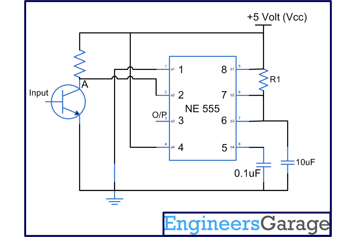
Image below shows the pin diagram of a 55 timer IC:
[[wysiwyg_imageupload:7743:]]
The circuit in this project uses an npn transistor T1 to achieve the above objective. 555 timer in monostable configuration is shown in the figure. Pin 2, which is the trigger pin of the IC is connected to the collector of T1. When no signal is present on the base the transistor T1, it is in the cut off state. As a result point “A” is high, thus making the pin 2 high and there is no output at pin 3 of the IC.
When the base gets a high signal, the transistor starts conducting and behaves like a closed switch. The point A gets connected to ground via emitter and hence the trigger pin goes low. When the trigger goes low a pulse is produced at the output pin. Here we have used a LED to show the output. The time period of the pulse is decided by the value of capacitor and resistor.
Circuit Diagrams
Project Components
Filed Under: 555 Timers, Electronic Projects

Questions related to this article?
👉Ask and discuss on Electro-Tech-Online.com and EDAboard.com forums.
Tell Us What You Think!!
You must be logged in to post a comment.