A constant current source is used to provide a constant current regardless of the input voltage and output load. These type of circuits are also used as a current limiter. Most electronic devices have a maximum current rating and if current above that rating is drawn by it, the device may get damaged or not work properly. Therefore a lot of times constant current power supplies are required to operate electronic devices. In this project, an adjustable constant current source which supplies 25 mA constant current at the output regardless of load resistance and the input voltage is designed.
The constant current of 25 mA in this circuit can be changed as per requirement by just changing the series resistance at the output of the circuit. The circuit designed in this project can be adjusted to provide a constant current up to 1.5 A. The circuit inputs AC voltage from main supplies and regulate it using LM317 voltage regulator IC. The current at the output is limited to 25 mA by a series resistance of 50 ohms at the output terminals of the circuit.
Components Required –

Fig. 1: List of Components required for Adjustable Constant Current Source
Block Diagram –

Fig. 2: Block Diagram of Adjustable Constant Current Source
Circuit Connections –
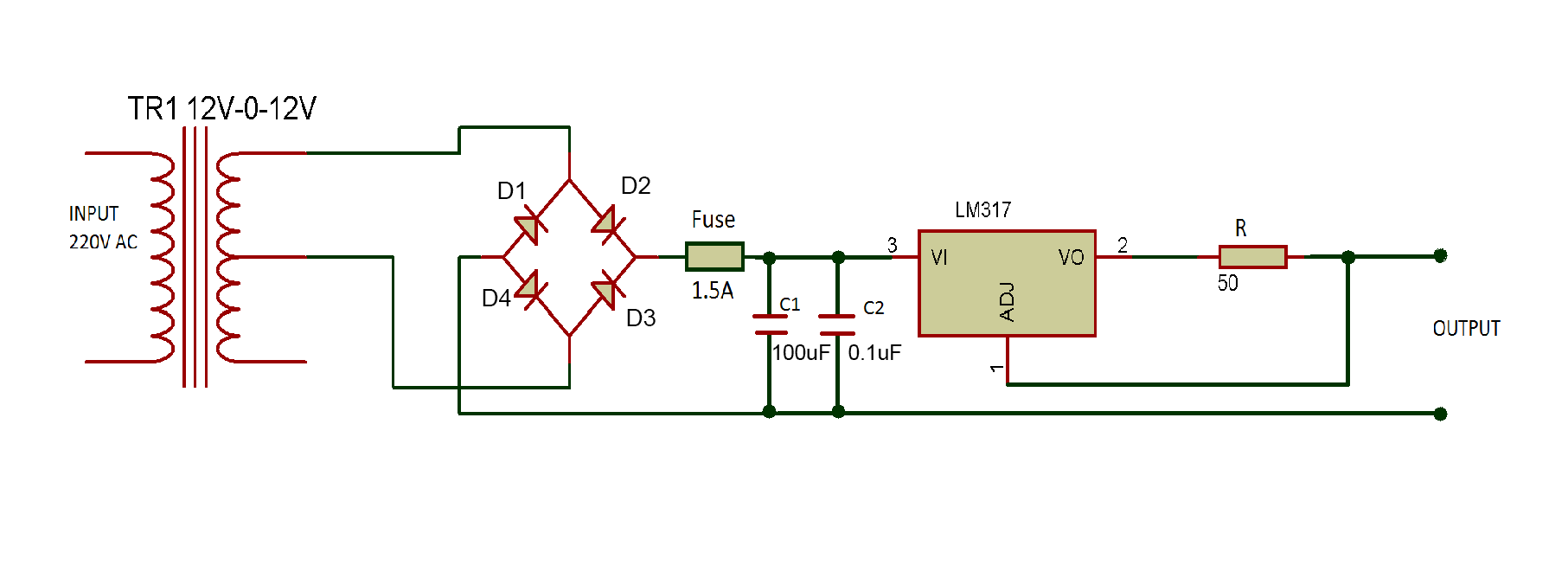
First of all, for stepping down the 230 V AC, a 12V – 0 -12V transformer is taken. One end of the secondary coil of the transformer and center tape of it are connected with a full-bridge rectifier. The full bridge rectifier is built by connecting four SR560 diodes to each other designated as D1, D2, D3 and D4 in the schematics. The cathode of D1 and anode of D2 is connected to one of the secondary coil and cathode of D4 and anode of D3 is connected to the center tape. The cathodes of D2 and D3 are connected from which one terminal is taken out from the output of rectifier and anodes of D1 and D4 are connected from which other terminal is taken out from the output from full-wave rectifier.
A fuse of 1.5A is connected at the output of the full-bridge rectifier and the output terminal of the full-bridge rectifier is connected to voltage input terminal of the LM-317 IC. The adjust pin of the voltage regulator IC is connected to the ground that is provided by the center tape of the transformer. The output voltage is drawn from the voltage output terminal of LM-317. A resistance of 50 ohms is connected in series to the voltage output terminal of LM-317 to limit the current. The output voltage is drawn from the voltage output terminal of the IC and the common ground.
How the circuit works –
The circuit operates by executing following operations –
1. AC to AC Conversion
2. AC to DC Conversion – Full Wave Rectification
3. Smoothing
4. Voltage regulation
5. Limiting Current
AC to AC conversion
The voltage of Main Supplies is approximately 220-230V AC which further needs to be stepped down to 12V level. To reduce the 220V AC to 12V AC, a step-down transformer with center taping is used. The use of center tap transformer allows to generate both positive and negative voltage at the input, however, only positive voltage will be drawn from the transformer. The circuit takes some drop in the output voltage due to resistive loss. Therefore a transformer of high voltage rating greater than the required 12 V needs to be taken. The transformer should provide 1.5 A current at the output. The most suitable step-down transformer that meets the mentioned voltage and current requirements is 12V-0-12V/2A. This transformer step downs the main line voltage to +/-12V AC, as shown in the below image.

Fig. 3: Circuit Diagram of 12-0-12V Transformer
AC to DC conversion – Full Wave Rectification
The stepped down AC voltage needs to be converted to DC voltage through rectification. The rectification is the process of converting AC voltage to DC voltage. There are two ways to convert an AC signal to the DC one. One is half wave rectification and another is full wave rectification. In this circuit, a full-wave bridge rectifier is used for converting the 24V AC to 24V DC. The full wave rectification is more efficient than half wave rectification since it provides complete use of both the negative and positive sides of AC signal. In full wave bridge rectifier configuration, four diodes are connected in such a way that current flows through them in only one direction resulting in a DC signal at the output. During full wave rectification, at a time two diodes become forward biased and another two diodes get reverse biased.

Fig. 4: Circuit Diagram of Full Wave Rectifier
During the positive half cycle of the supply, diodes D2 and D4 conduct in series while diodes D1 and D3 are reverse biased and the current flows through the output terminal passing through D2, output terminal and the D4. During the negative half cycle of the supply, diodes D1 and D3 conduct in series, but diodes D4 and D2 are reverse biased and the current flow through D1, output terminal and the D3. The direction of current both ways through the output terminal in both conditions remain the same.

Fig. 5: Circuit Diagram showing positive cycle of Full Wave Rectifier

Fig. 6: Circuit Diagram showing negative cycle of Full Wave Rectifier
The SR560 diodes are chosen to build the full wave rectifier because they have the maximum (average) forward current rating of 2A and in reverse biased condition, they can sustain peak inverse voltage up to 36V. That is why SR560 diodes are used in this project for full wave rectification.
Smoothing
As its name suggest it is the process of smoothing or filtering the DC signal by using a capacitor. A capacitor C1 of high value is connected to the output of rectifier circuit. As the DC which is to be rectified by the rectifier circuit has many AC spikes and unwanted ripples, so to reduce these spikes we use a capacitor. This capacitor acts as a filtering capacitor which bypasses all the AC through it to ground. At the output, the DC which is left is now smoother and ripples free. A small value of ceramic capacitor C2 is also used in parallel with C1 to reduce the overall ESR.

Fig. 7: Circuit Diagram of Smoothing Capacitor in Adjustable Constant Current Source
Voltage Regulation
LM317 is used for the voltage regulation. LM317 is a monolithic positive voltage regulator IC. Being monolithic, all the components are inbuilt on the same semiconductor chip making the IC small in size having less power consumption and low cost. The IC has three pins – 1) Input pin where maximum 40 V DC can be supplied, 2) Output pin which provides an output voltage in the range of 1.25 V to 37 V and 3) Adjust pin which is used to vary the output voltage corresponding to the applied input voltage. For input up to 40 V, the output can vary from 1.25 V to 37 V.
There is an In-built OPAM (Operational Amplifier) on the IC whose inverting input is connected with the adjustment pin. The non-inverting input is set by a band gap voltage reference whose voltage is independent of the temperature, power supply, and circuit loading. Therefore, LM317 gives a stable reference voltage of 1.25 V across its adjust pin. The reference voltage of 317 can be from 1.2 V to 1.3 V.
The LM317 has the following internally tolerable power dissipation –
Pout = (Maximum operating temperature of IC)/ (Thermal Resistance, Junction−to−Ambient + Thermal Resistance, Junction−to−case)
Pout = (150) / (65+5) (values as per the datasheet)
Pout = 2 W
Therefore, LM317 internally can sustain up to 2 W power dissipation. Above 2 W, the IC will not tolerate the amount of heat generated and will start burning. This can cause a serious fire hazard also. So heat sink is needed to dissipate the excessive heat from the IC.
Limiting Current
Due to the constant 1.25V reference voltage of the LM317, it provides a constant current at the output. By using this feature of 317, an adjustable constant current source can be designed. For setting the constant current at the output a resistance R is connected between the voltage output and adjustment pin of LM-317. In normal conditions when there is the constant demand of current at the output the 317 maintains a voltage of 1.25V at its adjust terminal. Therefore the voltage across R is also 1.25V. As the current demand changes at the output, it should also change the voltage drop across R but LM-317 adjusts the output voltage to compensate a constant 1.25V drop across resistance R.
Therefore, the voltage across R is always 1.25V and a constant current flows through it. This constant current can be calculated as follows –
Iout = 1.25/R
For changing the output constant current the value of series resistance R should be changed by replacing the resistor. The 317 IC can provide current up to 1.5A if the proper heat sink is applied to the IC. The IC can provide a minimum current of 10mA and maximum 1.5A.
So the minimum value of resistance R in the circuit is as follows –
Rmin = 1.25/ Imax
Rmin = 1.25/1.5
Rmin = 0.83 ohm
Therefore, for any resistance below 0.83 ohm the current will be greater than the 1.5A and IC will not be able to provide that much current.
The maximum value of resistance is as follows –
Rmax = 1.25/ Imin
Rmax = 1.25/0.01
Rmax = 125 ohm

Fig. 8: Circuit Diagram of Current Limiter
Testing and Precautions –
The following precautions need to be taken while assembling the circuit –
• The current rating of the step-down transformer, bridge diodes and voltage regulator ICs must be greater than or equal to the required current at the output. Otherwise, it will be unable to supply the required current at the output.
• For driving the high load at the output, heat sink should be mounted at the holes of the regulator. This will prevent the IC from blowing off due to heat dissipation.
• As the regulator IC can draw current up to 1.5A only, a fuse of 1.5A needs to be connected. This fuse will limit the current in the regulator up to 1.5A. For current above 1.5A, the fuse will blow off and this will cut the input supply from the circuit. This will protect the circuit and regulator ICs from current greater than 1.5A.
• The current drawn at the output should not be 1.5A, otherwise the voltage regulator IC will get damaged.
• The dropout voltage of LM317 IC is about 1.5V to 2.5V depending upon the output current. Thus input voltage must be 1.5V to 2.5V greater than the maximum voltage drop across the load. The voltage drop across the load can be calculated as follows –
V = I(constant current) * R(Load Resistance)
Once the circuit is assembled, plug it to main supplies and measure output voltage and current using a multimeter with different loads.
When a load of 50 ohms resistance is connected at the output terminals, the output current is measured to be 24.6 mA. Theoretically, output current is derived as follows –
output current = 1.25/R
Iout = 1.25/50
Iout = 25mA
So the percentage error of output current is as follows –
% Error = (Theoretical Observation – practical observation) *100 /practical observation
% Error = (0.025 – 0.0246)*100/0.0246
% Error = 1.6%
The power dissipation of the voltage regulator IC is as follows –
Pout = (Vin – Vout)*Iout
Pout = (12- 1.5)*0.0246
Pout = 0.25W
When a load of 25 ohms resistance is connected at the output terminals, the output current is measured to be 49.8 mA. Theoretically, output current is derived as follows –
output current = 1.25/R
Iout = 1.25/25
Iout = 50mA
So the percentage error of output current is as follows –
% Error = (Theoretical Observation – practical observation) *100 /practical observation
% Error = (0.050 – 0.0498)*100/0.0498
% Error = 0.4 %
The power dissipation of the voltage regulator IC is as follows –
Pout = (Vin – Vout)*Iout
Pout = (12- 1.7)*0.0498
Pout = 0.51W
Therefore with different values of R, different constant currents are obtained. Though from the above practical experience, power dissipation in the IC is found within the internal tolerable limits, it is still recommended to use a heat sink to aid cooling the IC and to increase the lifespan of it.
The circuit designed in this project can be used as a constant current LED driver, current limiter circuit, constant current battery charger, super-cap charger and constant current power supply.
Circuit Diagrams
Project Video
Filed Under: Featured Contributions
Filed Under: Featured Contributions

Questions related to this article?
👉Ask and discuss on EDAboard.com and Electro-Tech-Online.com forums.
Tell Us What You Think!!
You must be logged in to post a comment.