This project explains how to interface the SD card with an LPC1768. The ARM Cortex M3 runs on 3.3V power supply with a built in crystal frequency of 16 MHz. A 32GB SDSC card from Transcend is used in this particular project, but the code will work with most of the SD cards. The SD card is formatted with FAT32. The ultimate aim of this project is to create a file in the FAT32 file system of the SD card.
The SD card has been formatted as FAT32 before interfacing. The generalized code for the FAT32 is written to interface the SD card. Explanations of the FAT32 file system and how to access files from these file system is explained in this project.
For setting up the Environment for the development of ARM cortex M3 is well discussed in this article.

Fig. 1: SD Card Interfacing With LPC1768 Prototype
SD card is consisting of two basic semiconductor sections, a ‘memory core’ and a ‘SD card controller’. The ‘memory core’ is the flash memory region where the actual data of the file is saved. When we format the SD card a file system will be written into this region. Hence this is the region where the file system exists. The ‘SD card controller’ helps to communicate the ‘memory core’ with the external devices like microcontrollers. It can respond to certain set of standard SD commands and read or write data from the memory core in for the external device.
For more details refer the below article.
Interfacing SD Card with AVR Microcontroller.
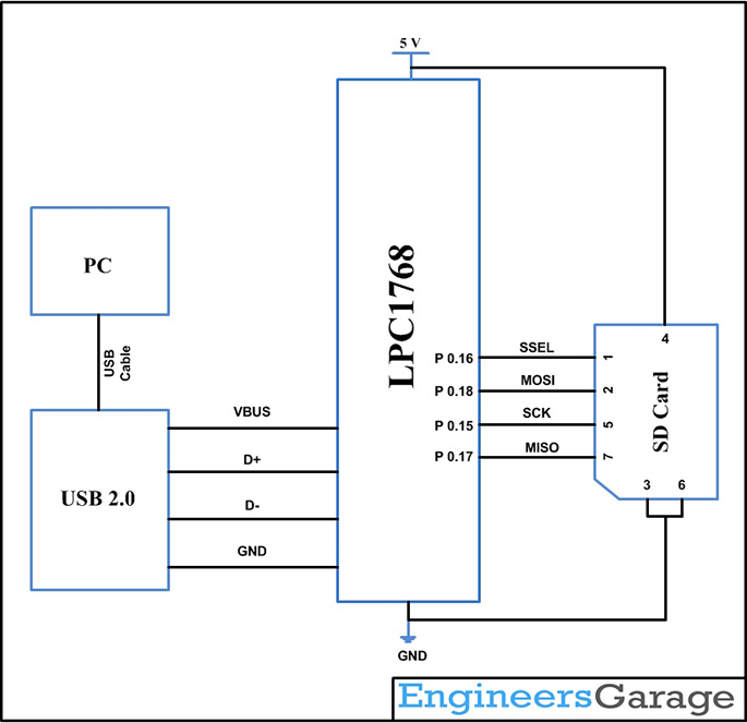
In this project the SPI bus is used for the serial interface. The Circuit diagram shows how to interface more than one SD card with a microcontroller. In this kind of interfacing the microcontroller is called the ‘Host’ and the SD card is called the ‘Slave’. The microcontroller initiates all the data transfers. The clock is also controlled by the microcontroller. The microcontroller is free to choose between the SD cards by asserting the respective CS (Chip Select) pin.
The data is transmitted from the microcontroller to the SD card using the MOSI (Master Output Slave Input) channel and the data is transferred by the SD card to the microcontroller using the MISO (Master Input Slave Output) channel.
The pin out of a SD card for the SPI interfacing mode is shown in the following figure.

Fig. 2: Pin Name And Description of SD Card for SPI Interfacing Mode

Fig. 3: Pin Diagram Of Sd Card
The circuit diagram for the serial interfacing of a SD card with the microcontroller including the level converter is shown in the circuit diagram tab.
LPC1768 SPI BLOCK:
POWERING THE SPI:
PCON register bits description:
|
Bit |
Symbol |
Description |
Reset value |
|
0 |
– |
Reserved. |
NA |
|
1 |
PCTIM0 |
Timer/Counter 0 power/clock control bit. |
1 |
|
2 |
PCTIM1 |
Timer/Counter 1 power/clock control bit. |
1 |
|
3 |
PCUART0 |
UART0 power/clock control bit. |
1 |
|
4 |
PCUART1 |
UART1 power/clock control bit. |
1 |
|
5 |
– |
Reserved. |
NA |
|
6 |
PCPWM1 |
PWM1 power/clock control bit. |
1 |
|
7 |
PCI2C0 |
The I2C0 interface power/clock control bit. |
1 |
|
8 |
PCSPI |
The SPI interface power/clock control bit. |
1 |
|
9 |
PCRTC |
The RTC power/clock control bit. |
1 |
|
10 |
PCSSP1 |
The SSP 1 interface power/clock control bit. |
1 |
|
11 |
– |
Reserved. |
NA |
|
12 |
PCADC |
A/D converter (ADC) power/clock control bit. |
0 |
|
13 |
PCCAN1 |
CAN Controller 1 power/clock control bit. |
0 |
|
14 |
PCCAN2 |
CAN Controller 2 power/clock control bit. |
0 |
|
15 |
PCGPIO |
Power/clock control bit for IOCON, GPIO, and GPIO interrupts. |
1 |
|
16 |
PCRIT |
Repetitive Interrupt Timer power/clock control bit. |
0 |
|
17 |
PCMCPWM |
Motor Control PWM |
0 |
|
18 |
PCQEI |
Quadrature Encoder Interface power/clock control bit. |
0 |
|
19 |
PCI2C1 |
The I2C1 interface power/clock control bit. |
1 |
|
20 |
– |
Reserved. |
NA |
|
21 |
PCSSP0 |
The SSP0 interface power/clock control bit. |
1 |
|
22 |
PCTIM2 |
Timer 2 power/clock control bit. |
0 |
|
23 |
PCTIM3 |
Timer 3 power/clock control bit. |
0 |
|
24 |
PCUART2 |
UART 2 power/clock control bit. |
0 |
|
25 |
PCUART3 |
UART 3 power/clock control bit. |
0 |
|
26 |
PCI2C2 |
I2C interface 2 power/clock control bit. |
1 |
|
27 |
PCI2S |
I2S interface power/clock control bit. |
0 |
|
28 |
– |
Reserved. |
NA |
|
29 |
PCGPDMA |
GPDMA function power/clock control bit. |
0 |
|
30 |
PCENET |
Ethernet block power/clock control bit. |
0 |
|
31 |
PCUSB |
USB interface power/clock control bit. |
0 |
Fig. 4: Bits Description Of PCON Register For POWERING SPI In LPC1768
Following reset the PCSPI (Power Clock Control Bit to SPI) bit is set and the ADC is enabled.
SELECTING CLOCK FOR SPI:
By assuming that the main clock for the LPC1768 has been programmed. Each LPC1768 peripheral including the ADC has a clock derived from the main clock as illustrated.
Peripheral Clock Divider
As shown in the below block the frequency of the peripheral clock is determined by two bits in the PCLKSEL registers. ADC is included in PCLKSEL0. With the NXP LPC1768 the peripheral clocks are always active. Following RESET PCLKSEL registers are cleared setting the peripheral clock frequency to CCLK/4 to all the peripherals. The user will have a choice of frequency which can be determined by two bits for each peripherals among the peripheral clock selection registers PCLKSEL0 and PCLKSEL1. By default at reset all values are 00 ie CCLK/4.
|
00 |
PCLK_peripheral = CCLK/4 |
|
01 |
PCLK_peripheral = CCLK |
|
10 |
PCLK_peripheral = CCLK/2 |
|
11 |
PCLK_peripheral = CCLK/8, except for CAN1, CAN2, |
Fig. 5: Bit Combination Of PCLKSEL Registers For Clock Selection
|
Bit |
Symbol |
Description |
|
1:0 |
PCLK_WDT |
Peripheral clock selection for WDT. |
|
3:2 |
PCLK_TIMER0 |
Peripheral clock selection for TIMER0. |
|
5:4 |
PCLK_TIMER1 |
Peripheral clock selection for TIMER1. |
|
7:6 |
PCLK_UART0 |
Peripheral clock selection for UART0. |
|
9:8 |
PCLK_UART1 |
Peripheral clock selection for UART1. |
|
11:10 |
– |
Reserved. |
|
13:12 |
PCLK_PWM1 |
Peripheral clock selection for PWM1. |
|
15:14 |
PCLK_I2C0 |
Peripheral clock selection for I2C0. |
|
17:16 |
PCLK_SPI |
Peripheral clock selection for SPI. |
|
19:18 |
– |
Reserved. |
|
21:20 |
PCLK_SSP1 |
Peripheral clock selection for SSP1. |
|
23:22 |
PCLK_DAC |
Peripheral clock selection for DAC. |
|
25:24 |
PCLK_ADC |
Peripheral clock selection for ADC. |
|
27:26 |
PCLK_CAN1 |
Peripheral clock selection for CAN1.[1] |
|
29:28 |
PCLK_CAN2 |
Peripheral clock selection for CAN2.[1] |
|
31:30 |
PCLK_ACF |
Peripheral clock selection for CAN acceptance filtering.[1] |
Fig. 6: Bit Values And Description Of PCLKSEL Register In LPC1768 ‘s SPI
Selecting the SPI function to GPIO:
The below block diagram shows the SPI input pins multiplexed with other GPIO pins. The SPI pin can be enabled by configuring the corresponding PINSEL register to select SPI function.
When the SPI function is selected for that pin in the Pin Select register, other Digital signals are disconnected from the SPI input pins.
|
SPI PINS |
Port Pin |
Pin Functions |
Associated PINSEL Register |
|
SCK |
P0.15 |
0-GPIO, 1-TXD1, 2-SCK0, 3-SCK |
30,31 bits of PINSEL0 |
|
SSEL |
P0.16 |
0-GPIO, 1-RXD1, 2-SSEL0, 3-SSEL |
0,1 bits of PINSEL1 |
|
MISO |
P0.17 |
0-GPIO, 1-CTS1, 2-MISO0, 3-MISO |
2,3 bits of PINSEL1 |
|
MOSI |
P0.18 |
0-GPIO, 1-DCD1, 2-MOSI0, 3-MOSI |
4,5 bits of PINSEL1 |
Fig. 7: SPI Input Pins Multiplexed With GPIO Pins In LPC1768
SPI REGISTERS:
The registers associated with LPC1768 ADC are
-
SPCR -> SPI Control Register : used to configure SPI
-
SPSR -> SPI status Register : Check the status.
-
SPDR – > SPI Data Register : contains received data or data to be transmitted
-
SPCCR -> SPI Clock Counter Register : used to control master SCK frequency
SPI REGISTER CONFIGURATION:
SPCR (SPI Control Register)
|
Bit |
Symbol |
Description |
Reset value |
|
1: 0 |
– |
Reserved, user software should not write ones to reserved bits. |
NA |
|
2 |
BIT ENABLE |
0-> The SPI controller sends and receives 8 bits of data per transfer. 1-> The SPI controller sends and receives the number of bits selected by bits 11:8 |
0 |
|
3 |
CPHA |
0-> Data is sampled on the first clock edge of SCK. A transfer starts and ends with activation and deactivation of the SSEL signal. 1-> Data is sampled on the second clock edge of the SCK. A transfer starts with the first clock edge, and ends with the last sampling edge when the SSEL signal is active. |
0 |
|
4 |
CPOL |
Clock polarity control. 0-> SCK is active high. 1-> SCK is active low. |
0 |
|
5 |
MSTR |
Master mode select. 0-> The SPI operates in Slave mode. 1-> The SPI operates in Master mode. |
0 |
|
6 |
LSBF |
LSB First controls which direction each byte is shifted when transferred. 0-> SPI data is transferred MSB (bit 7) first. 0-> SPI data is transferred LSB (bit 0) first. |
0 |
|
7 |
SPIE |
Serial peripheral interrupt enable. 0-> SPI interrupts are inhibited. 1-> A hardware interrupt is generated each time the SPIF or MODF bits are activated. |
0 |
|
11:8 |
BITS |
When bit 2 of this register is 1, this field controls the number of bits per transfer: 1000-> 8 bits per transfer 1001-> 9 bits per transfer 1010-> 10 bits per transfer 1011-> 11 bits per transfer 1100-> 12 bits per transfer 1101-> 13 bits per transfer 1110-> 14 bits per transfer 1111-> 15 bits per transfer 0000-> 16 bits per transfer |
0000 |
|
31:12 |
– |
Reserved, user software should not write ones to reserved bits. |
NA |
Fig. 8: Bit Configuration of SPCR Control Register in SPI
SPSR (SPI status Register)
The S0SPSR register controls the operation of SPI0 as per the configuration bits setting.
|
Bit |
Symbol |
Description |
Reset value |
|
2:0 |
– |
Reserved, user software should not write ones to reserved bits. |
NA |
|
3 |
ABRT |
Slave abort. When 1, this bit indicates that a slave abort has occurred. This bit is cleared by reading this register. |
0 |
|
4 |
MODF |
Mode fault. when 1, this bit indicates that a Mode fault error has occurred. This bit is cleared by reading this register, then writing the SPI0 control register. |
0 |
|
5 |
ROVR |
Read overrun. When 1, this bit indicates that a read overrun has occurred. This bit is cleared by reading this register. |
0 |
|
6 |
WCOL |
Write collision. When 1, this bit indicates that a write collision has occurred. This bit is cleared by reading this register, then accessing the SPI Data Register. |
0 |
|
7 |
SPIF |
SPI transfer complete flag. When 1, this bit indicates when a SPI data transfer is complete. When a master, this bit is set at the end of the last cycle of the transfer. When a slave, this bit is set on the last data sampling edge of the SCK. This bit is cleared by first reading this register, then accessing the SPI Data Register. Note: this is not the SPI interrupt flag. This flag is found in the SPINT register. |
0 |
|
31:8 |
– |
Reserved, user software should not write ones to reserved bits. |
NA |
Fig. 9: Bit Value Of SPSR Status Register For Operation Control In SPI
SPDR (SPI Data Register )
|
Bit |
Symbol |
Description |
Reset value |
|
7:0 |
DataLow |
SPI Bi-directional data port. |
0x00 |
|
15:8 |
DataHigh |
If bit 2 of the SPCR is 1 and bits 11:8 are other than 1000, some or all of these bits contain the additional transmit and receive bits. When less than 16 bits are selected, the more significant among these bits read as zeroes. |
0x00 |
|
31:16 |
– |
Reserved, user software should not write ones to reserved bits. |
NA |
Fig. 10: Bit value of SPDR Data Register in SPI
SPCCR (SPI Clock Counter Register )
|
Bit |
Symbol |
Description |
Reset value |
|
7:0 |
Counter |
SPI0 Clock counter setting. |
0x00 |
|
31:8 |
– |
Reserved, user software should not write ones to reserved bits. |
NA |
Fig. 11: Bit Value Of SPCCR Clock Counter Register In SPI
Create a project using Keil uvision4 for LPC1768 Microcontroller:
In this section, we will start creating a project in Keil MDK we have already installed Keil µVision and Co-MDK Plug-in + CoLinkEx Drivers required for the CoLinkEx programming adapter. You can start by downloading the project files and kick start your practical experiment.
Code Description:
First we have to initialize and mount the SD card, this can be done by following functions.
status = disk_initialize(0);
result = f_mount(0,&drive);
In this example creating and writing to a text file will be explained. First the file has to be opened. The command for this is result = f_open(&file, “test.txt”, FA_CREATE_NEW);
There are different modes of opening a file. The modes are:
FA_READ
FA_WRITE
FA_READ and FA_WRITE are self-explaining. There are some more commands. Those are explained on the bottom of the tutorial. A correct command to open a file called “test.txt” for reading is:
result = f_open(&file1, “test.txt”, FA_READ );
After a file is opened it is possible to read and write from that file. The command to read data from the file is: result = f_read(File, Buffer, bytes to read, bytes done); File is the opened file. Buffer is a buffer where all the data will be placed in. Buff is a variable declared earlier for this. Bytes to read is the amount of bytes that will be read from the file. This can be a variable or just a number. Bytes done is a variable that will contain the number of bytes that have been read successfully.
To write to a file it has to be opened with FA_WRITE. The command to write to a file is: result = f_write(File, Data to be written, Number of byte to write, Bytes done); File is the opened file. Data to be written can be the Buff variable or just a string of text. Number of bytes to write can be a variable or just a number. Bytes done is a variable that will contain the number of bytes that have been read successfully. A correct command to write a string of text to a file is:
result = f_write(&file1, “Hello world “, 11, &s2);
When you are done with reading/writing to a file ALWAYS close the file! Not doing this can result in hard to find bugs. The command to close a file is result = f_close(file1);
Project Source Code
###The codes are linked in Description ###
Circuit Diagrams
Project Video
Filed Under: ARM.
Filed Under: ARM.

Questions related to this article?
👉Ask and discuss on EDAboard.com and Electro-Tech-Online.com forums.
Tell Us What You Think!!
You must be logged in to post a comment.