In the previous tutorial, we learned how to design an audio crossover, using high and low-pass audio filters. Next, let’s design an audio equalizer.
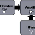
Equalization is the process of adjusting frequency elements in sound. An equalizer (EQ) is an audio filter that isolates certain frequency components from an audio signal, either boosting or lowering them.
EQs are widely used in audio systems, including while recording or with amplifiers and mixers. They’re typically used to correct or adjust the response of the speakers, amps, microphone, or even a room’s acoustics. They’re the cornerstone of any DJ’s audio system.

A three-band audio equalizer.
In an EQ system, audio signals are split into different frequency bands. These bands offer greater control over the frequency ranges and each has a separate slider, which controls the gain of the input audio signal. A current summer, then, combines the frequency bands with the updated audio track.
There are two types of equalizers:
1. Parametric equalizer: typically used in mixing and recording studios as these EQs offer more precision. They let a user control the bandwidth (also known as Q or quotient of change), the center frequency, and the frequency levels (the gain) via different knobs.

A parametric audio equalizer.
2. Graphic equalizer: has a fixed bandwidth and center frequency but the gain of a frequency band can be adjusted via different sliders. The greater the amount of sliders on this EQ means the greater amount of control over a wider range of frequencies.

A graphic audio equalizer.
Equalizers can be designed using audio filters or integrated chips (such as an LA-3600, which is a five-band equalizer IC).
For this project, we’ll design a three-band, graphic equalizer circuit using audio filters. So, it will have low, high, and band-pass filter circuits to separate the low, high, and mid-range frequencies of the audio signal. The circuits will be active filters using an operational amplifier (op-amps).
The gain for each frequency band will be regulated using variable resistors, connected at the filter circuits’ input. The different frequency components will be combined at the filters’ output stage and connected to an LM386-based power amplifier circuit. The amplifier circuit will boost the combined audio signal and direct it to a speaker.
To properly test this EQ, we’ll analyze the frequency response curve of the audio filters. The curve will be drawn by plotting the voltage levels of the audio signal with respect to the frequencies. A function generator will be used as the input source to produce sinusoidal waves at different frequencies.
We’ll be using some common terms associated with audio amplifiers or audio filters, such as gain, cut-off frequency, bandwidth, and the quality factor. We covered some of these in the previous tutorial: Understanding the filters.
Components required


Our equalizer is designed for using three audio filters:
- A high-pass filter for separating the high-frequency elements
- A band-pass filter for separating the mid-range frequency elements
- A low-pass filter for separating low-frequency elements
The gain for the different frequency bands is controlled through variable resistors, connected at the filters’ input. Afterward, the frequency bands are combined into one audio signal and passed to a power amplifier and speaker.
The equalizer circuit is built by assembling the following components…
A power supply – A dual-power supply is used to power the filter circuits, using two 9V batteries. As a DC source is required to bias the op-amps, the batteries provide the negative and positive voltages.
These batteries’ positive and negative supply voltages are provided to the operational amplifiers used in all of the filters.
- For the negative voltage, the cathode of one of the batteries is connected to the op-amp’s negative supply pin and that battery’s anode is connected to the common ground.
- For the positive voltage, the anode of the other battery is connected to the op-amp’s positive supply pin and that battery’s cathode is connected to the common ground.

A circuit diagram of the dual-power supply for the active high and low-pass filters.
Audio source – The audio input is provided from a smartphone, using a 3.5mm jack. The jack should have three wires: one to ground, one for the left channel, and a third for the right channel. The wires that connect to the channels are used for the stereo systems.
In this system, the audio signal from both channels is transmitted with a phase difference of 180 degrees. The phase-shifted audio signals are combined to produce a noise-free audio signal, which is called a balanced audio system.
In our circuit, however, only one of the channels is used for the audio source. The jack’s ground wire is connected to the common ground. So, this audio system will be unbalanced and the audio source will be connected as a single or mono-source channel.

A 3.5mm audio jack.
The audio signal passes through the capacitor. Its impedance is inversely proportional to the frequency and the capacitance — so, the lower the frequency, the higher the impedance and vice-versa.
The high-frequency element of the audio signal will, therefore, have less impedance and easily pass through the capacitor and to the amplifier’s non-inverting input. The low-frequency element of the signal will contain a greater level of impedance. It’s bypassed through the resistor that’s connected to the ground.
The impedance of the capacitor can be determined using this equation:
(Impedance), Xc= 1/ (2π*f*C)
The high-pass filter is designed using a capacitor (“C1” in the circuit diagram) of 100 nF and a resistor (“R2”) of 3.2 kilo-ohms. Using these values for the capacitor and resistor, the cut-off frequency of the filter can be calculated as follows:
FH= 1/ (2πR2C1)
FH= 1/ (2π*3.2k*100n)
FH= 500Hz (approx.)
The RC network forms a passive, high-pass filter. Through this network, the filtered audio signal — which now carries only high-frequency signals — is passed to the op-amp’s non-inverting pin.

A circuit diagram of an LM741 op-amp in an active, high-pass filter.
For this project, we’re using the LM741 IC op-amp. The LM741 is a general-purpose, operational amplifier with a low-input impedance (megaohms), compared to a FET op-amp, which has a high-input impedance (in gigaohms).
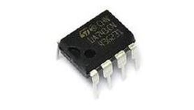
The LM741 IC.
The output impedance of the 741 should, ideally, be zero but it’s typically about 75 ohms. The maximum supply current of the 741 IC is about 2.8 mA, with a supply voltage up to +/- 18V.
The IC has the following pin configuration…
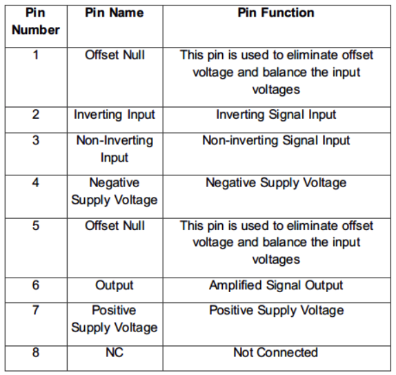

The IC has input and output overload protection and has zero latch-up when the common-mode range is exceeded. The IC can be provided a positive or negative supply voltage up to 22V and an input signal voltage (amplitude) up to 15V. Generally, it must be provided a positive or negative voltage of at least 10V.
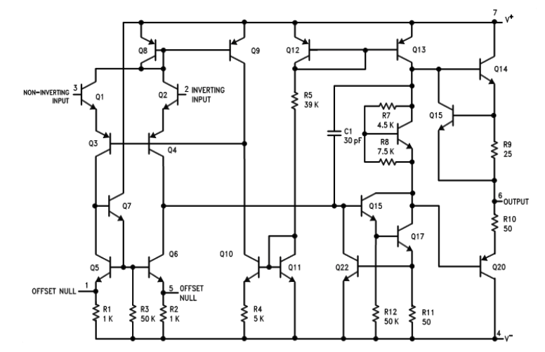
The internal circuit diagram of an LM741 IC op-amp.
The LM741 can be configured as an open or closed-loop amplifier, and as an inverting or non-inverting amplifier.
In this circuit, the LM741 IC has been used as a non-inverting amplifier. The input signal from the passive, high-pass filter is connected to the IC’s non-inverting input pin (pin 3). A 22 kilo-ohm resistor (“R5” in the circuit diagram) is connected between the IC’s pins 6 and 2, providing negative feedback. The inverting pin (pin 2) is grounded via a 2.2 kilo-ohm resistor (“R3”).
The gain of the amplifier is set by these resistors and can be calculated as follows:
Gain = (R5/R3)
= 22/2.2 kilo ohms
= 10
As a result, the high-frequency element of the audio signal is amplified 10 times compared to the input audio signal. The op-amp’s output is drawn from the IC’s pin 6, which is connected to one of the speaker’s wires.
Low-pass filter – An active first-order, low-pass filter is connected in the circuit. For this filter, the audio input is passed to the op-amp’s non-inverting pin via an RC network. The audio signal passes through the resistor, which has a frequency-independent response. The high-frequency elements of the audio signal are bypassed through a capacitor to the ground.
The impedance of the capacitor is inversely proportional to the frequency and its capacitance — so the lower the frequency, the higher the impedance and vice-versa. The high-frequency elements of the audio signal, therefore, experience less impedance and are easily bypassed through the capacitor to the ground. The low-frequency elements of the audio signal experience more impedance and cannot bypass through the capacitor.
The impedance of a capacitor can be provided with this equation:
(Impedance), Xc= 1/ (2π*f*C)
The low-pass filter is designed using a capacitor (“C2” in the circuit diagram) of 100 nF and a resistor (“R1”) of 3.2 kilo-ohms. Given these values of the capacitor and resistor, the cut-off frequency of the filter can be calculated as follows:
FH= 1/ (2πR2C1)
FH= 1/ (2π*3.2k*100n)
FH= 500 Hz (approx.)
The RC network forms a passive, low-pass filter. Through the network, the filtered audio signal — which now carries only low-frequency elements — is passed to the op-amp’s non-inverting pin.

A circuit diagram of a 741 op-amp used with an active, low-pass filter.
In this low-pass filter circuit, the LM741 IC is used as a non-inverting amplifier. The input signal from the filter is connected with the IC’s non-inverting input pin (pin 3).
As there’s no feedback circuit, the gain of the OPAM will be unity. However, there is a variable resistor (“RV1” in the circuit diagram), which is connected at the low-pass filter’s input. By adjusting this variable resistor, the voltage level of the input audio signal is increased or decreased.
The low-frequency element of the audio signal will be proportional to the voltage level of the input signal since the gain of the op-amp is unity. As such, the gain or strength of the low-frequency band can be adjusted using the RV1 variable resistor, which is typically mounted to a knob on the equalizer.
The output from the op-amp is drawn from the IC’s pin 6, which is connected to the power amplifier’s input.
Band-pass filter – An active, second-order band-pass filter is connected in the circuit. It’s designed with a center frequency of 1 kHz and a bandwidth of 1.5 kHz.
A band-pass filter consists of a high-pass filter connected in series with a low-pass filter. Note:
- The cut-off frequency of the high-pass is the lower cut-off frequency of the band-pass filter.
- The cut-off frequency of the low-pass is the higher cut-off frequency of the band-pass filter.
- Only the frequencies between the two high and low-pass cut-off frequencies are allowed to pass at the output.
This band-pass filter has a frequency band between 500 Hz and 1.5 kHz.
As seen in the circuit diagram, a low-pass filter with a resistor of 1.5K ohms (“R2”) and a capacitor of 100 nF (“C3”) are connected in series with the high-pass filter. It uses a capacitor of 100 nF (“C2”) and a resistor of 3K ohms (“R3”).
The LM741 IC is used for the op-amp as a non-inverting amplifier. The input signal from the passive band-pass filter is applied at the IC’s non-inverting input pin (pin 3).

A circuit diagram of the 741 op-amp-based, active band-pass filter, with an adjustable volume feature.
This is the second order called the key band-pass filter. It only passes the frequency which is in its cut-off frequency range.
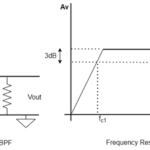
The band-pass filter has two cut-off frequencies — the lower and the upper cut-off frequencies. The center frequency and the bandwidth provide these two frequency ranges as shown in the curve below…

A graph showing a typical frequency curve of a band-pass filter.
In this circuit, the capacitance of the “C2” and “C3” capacitors is the same. The resistance of “R2” is also the same as the feedback of resistor “R4.”
The center frequency (fc) of this band-pass filter can be calculated as follows:
Fc= 1/ (2πRC)
Fc= 1/ (2π*1.5k*100n)
Fc=1 kHz (approx.)
The resistor network (“R6” and “R7”) is responsible for the gain of the amplifier. For the non-inverting amplifier configuration, the gain can be calculated using this equation:
G = (1+R7/R6)
G = (1 + 1k/1k) = 2
The quality factor for this configuration is calculated as follows:
Q =1/(3-G)
So, Q = 1
The bandwidth of this band-pass filter can be calculated as follows:
Bandwidth =fc/Q
So, Bandwidth = 1.5 kHz
From the frequency curve graph, it can be seen that the lower and upper cut-off frequencies of this filter are:
- Lower cut-off frequency, fL = 500Hz
- Upper cut-off frequency, fH = 1.5 kHz
The frequency (between 500 Hz and 1.5 kHz) is passed through the band-pass filter with a voltage gain of two. There’s a variable resistor (“RV2”), which is connected at the band-pass filter’s input. By adjusting this variable resistor, the voltage level of the input audio signal is increased or decreased.
The mid-frequency component of the audio signal will be two times the voltage level of the input signal since the op-amp’s gain is two. As such, the gain or strength of the mid-frequency band will be amplified by two and can be adjusted using the variable resistor “RV2.”
This variable resistor is typically mounted to a knob on the equalizer. The output from the op-amp is drawn from the IC’s pin 6, which is connected to the power amplifier’s input.
Power amplifier – The LM386 IC is used as the summer and non-inverting power amplifier in this circuit. The summer is responsible for adding the input signal and providing the output.
The three frequency band are combined and amplified by the 386 IC. It has an internal gain of 26 dB when pins 1 and 5 are left open, which means that the input signal is amplified by a factor of 20.

The LM-386 IC.
Speaker – A speaker with a 10-watt power rating and 8-ohm impedance is used as load at the output of the amplifier.
The speaker is connected at the IC’s pin 5, which is the LM386’s output pin. The ground wire of the speaker is connected to the common ground. An RC network includes a 10-ohm resistor (“R8” in the circuit diagram) and a 100 nF capacitor (“C6”), which is connected before the speaker.
This is called a “Zobel network.” It ensures that the impedance of the speaker provides steady resistance for the amplifier after the output. This stabilizes the frequency and oscillations at the output.
If the “C6” capacitor C6 and “R1” resistor were interchanged, it would be no longer form a Zobel network, but the output impedance would still remain constant.
The LM386’s pin 7, which is the “bypass terminal pin” is grounded with a capacitor (“C5”), which is important for improving the stability of the amplifier’s output.

The following precautions must be taken when assembling this circuit:
1. Only use speakers that are equivalent to the amplifier’s output — or of a high-power rating.
2. Avoid clipping the output signal as it may damage the speakers.
3. Always place the components as close as possible to reduce the noise in the circuit.
4. The 386 IC starts heating up when it delivers at high power, so it’s recommended to first apply a heat paste on its surface, which will also increase its lifespan.
5. The bread board produces a lot of noise and loose components, so it’s recommended to make this circuit on PCB for clear, distortion-free noise.

A prototype of a three-band audio equalizer.
How the circuit works
An audio signal is taken from a smartphone that’s connected through a 3.5mm jack to a single channel. This signal is passed through high, low, and band-pass filter circuits that each have variable resistors at their input. The resistors adjust the input signal levels and the filters adjust the gain for each frequency band, accordingly.
For example, the high-pass filter separates the high-frequency elements (above 1.5 kHz) and delivers them to the power amplifier with a unity gain. The low-pass filter separates the low-frequency elements (below 500 Hz), delivering them to the power amplifier with a unity gain. The band-pass filter separates the mid-frequency elements (from 500 Hz to 1.5 kHz) and passes them onto the power amplifier with a voltage gain of two.
All of the frequency elements are, then, combined at the LM386’s input and amplified by 20 due to the IC’s programmed set gain of 26 dB. The output of the power amplifier is directed to a speaker to regenerate the sound.
By adjusting the variable resistance at the input of the filter circuits, the gain of the three frequency bands can be altered. This can be used to reduce noise or to create special sound effects from the original audio.

A prototype of active high, band, and low-pass filter.
Testing the circuit
The EQ can be tested by examining the performance of the filter circuits by using the function generator as the input source. It generates a sine wave of constant amplitude and variable frequency.
Since an audio signal is, essentially, a sine wave, a function generator can be used instead of using a microphone or other type of audio source.
Note: a speaker is not used as the load because it’s resistive and inductive. At different frequencies, its inductance changes which, in turn, changes the impedance (the “R” and “L” combination). So, the use of a speaker as the load at the amplifier’s output could give false or non-standard results.
Instead, we’ll use a dummy load that’s purely resistive. As resistance does not change with the frequency, it can be considered a reliable load independent of the frequency of the input audio signal.
The peak-to-peak amplitude of the signal from the function generator should be set to 100 mV, with a resistive load of 10 ohms connected at the output (instead of the speakers). The cut-off frequency of the high-pass filter must be 1.59 kHz and the low-pass filter must be 500 Hz. The center frequency of the band-pass filter must be 1 kHz, with a bandwidth between 500 Hz and 1.5 kHz. The signal gain from the power amplifier must be 20 (26 dB).
Based on our testing, the following frequency response of the high, band, and low-pass filters were observed:


The frequency response of a low-pass audio filter.

The frequency response of a band-pass audio filter.

The frequency response of a high-pass audio filter.
The frequency curve for the high, low, and band-pass filters can be more precisely plotted by taking voltage-level readings for a greater number of frequencies.
In this tutorial, we designed a three-band graphic audio equalizer that allows boosting or altering audio signals into high (above 1.5 kHz), low (below 500 Hz), and mid-range (from 500 Hz to 1.5 kHz) frequencies.
The output power of this equalizer is 700 mW and the voltage gain is 26 dB. This equalizer circuit can be used in DJ systems and for mixing soundtracks.
In the next tutorial, we’ll learn how to design an audio mixer.
You may also like:
Project Video
Filed Under: Audio, Tutorials
Filed Under: Audio, Tutorials

Questions related to this article?
👉Ask and discuss on Electro-Tech-Online.com and EDAboard.com forums.
Tell Us What You Think!!
You must be logged in to post a comment.