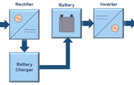
The main source of power is usually the AC Mains. The Mains Supply is used to charge a battery through the charger circuit. The battery provides the power backup when the mains supply is cut off. A battery stores electrical energy in the form of DC current. The power backup is provided by connecting the load circuit to the inverter. The inverter draws the power from the charged battery on power failure, converts back the DC power to AC power and provides power backup to the load. This is how any basic UPS works.
Designing an Offline UPS – Part (12 /17)

In the previous tutorial, Online UPS was assembled from its basic building blocks like Lead Acid battery Charger, Square Wave Inverter and Modified Sine Wave Inverter. Now in this tutorial, offline UPS will be designed. The Offline UPS is one of the topologies of UPS (Uninterruptible Power Supply). In UPS system, the term topology refers to the switching mechanism of the UPS system. Contrary to online UPS, in offline UPS, the load circuit is initially directly powered by the AC mains. On the failure of power supply, the power failure is detected by a switching circuit and the power is provided to the load through the battery and inverter after the power failure has already occurred. So, in the offline UPS, the load experiences the power cutoff once before it receives the power backup from the UPS.
Testing IR2110 Gate Driver IC- ( Part 14/17)
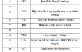
In the previous tutorial, it was discussed that for driving a MOSFET as high side switch, a gate driver circuit needs to be used. The IR2110 IC is one of the high speed and high voltage gate driver ICs for IGBT and power MOSFET. The IC is having independent low and high side output channel. By using a single IC, a half bridge circuit can be operated in which one MOSFET is in high side configuration and another one is in the low side configuration. For driving the high side MOSFET, this IC uses a bootstrap circuit which otherwise could have to be designed externally. Before using this IC for driving the half or full bridge circuit, it is necessary to test the faultiness of the IC. A faulty IC can give unstable output and may blow up the MOSFET or other components in the circuit. In this tutorial, the method to test the IR2110 IC is discussed.
Designing Gate Driver Circuit and Switching Mechanism for Modified Sine Wave Inverter – (Part 9/17)
In the previous tutorial, basic operation of a modified sine wave inverter was discussed. It was mentioned in the previous tutorial that the H-bridge MOSFET circuit of the quasi sine wave inverter cannot be directly interfaced with the microcontroller circuit. There is a need of a Gate driver circuit as an intermediate circuit between the microcontroller and the H-bridge MOSFET circuit. The H-bridge MOSFET circuit generates a modified sine wave by switching the MOSFETs in a sequential manner with predetermined delay. This sequential switching of the MOSFETs in the previous tutorial was explained with the help of a truth table and circuit diagrams.
How to reduce Switching Time of a Relay – (Part 15/17)
The relays are commonly used for switching purpose. There are many types of relays like electromagnetic relays, thermal relays, reed relay, solid state relay and hybrid relay. A relay is basically an electronically operated mechanical switch meant to be used for switching. The electromagnetic relays are also of many types like attraction type relay, induction type relay and magnetic latching relay. This tutorial is concerned about the magnetic latching relays which are to be used to switch the load between two DC power sources. The switching from one DC source to other takes some time, so it cuts the supply to the load for a short duration of time. This tutorial discusses about reducing the switching time, so that, the load does not experience any interruption during the transition phase of the relay.
Designing square wave inverter for UPS (Part – 6/17)
The square wave inverter is easy to design and suitable for less sensitive electronic devices. For more sensitive electronics, the supply from square wave inverter can result into noise. In this tutorial, a square wave inverter is designed which will input power from a battery and output a square AC waveform. An Inverter should generate an AC signal at the output but that signal is not necessarily an exact sine wave. A square wave can also be considered as an AC signal which can be used to drive less sensitive AC devices.
Designing Switching Mechanism with Step Up Transformer for Square Wave Inverter (Part- 7/17)

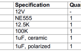
In the previous tutorial, a square wave generator was designed having a symmetric output waveform having 50 Hz frequency and 12 V peak to peak voltage. The square wave generator designed using 555 timer IC was meant to provide input square wave in the inverter circuit. Now, it is time to complete the square wave inverter circuit by adding a switching mechanism and step up transformer in the previous designed circuitry. The square wave generated from the 555 IC based circuit has peak to peak voltage of 12 V. This voltage needs to be stepped up using a step up transformer. So a step up transformer of 12V-0-12V rating is used for this purpose. But not only the voltage need to be simply stepped up, there is also a need for switching mechanism which allows drawing power from the inverter on power failure.
Designing 250 Milli Watt Audio Power Amplifier – 2/9

In the previous tutorial, basics of audio amplifiers were discussed. It has been already mentioned that on the basis of application, there are two types of audio amplifiers – 1) Pre-Amplifier2) Power Amplifier The pre-amplifiers are used to level up the audio signals from a microphone or audio source to standard voltage levels while the power amplifiers are generally used at the output stage of the audio systems to boost audio signals before they are reproduced by the speakers. In this tutorial, a power amplifier with 250 Milli-Watt output power will be designed.
Designing 1 Watt Audio Power Amplifier – 3/9

In the previous tutorial, a 250 Milli Watt Audio Power Amplifier was designed using LM-386 power amplifier IC. On the basis of application, the audio amplifiers can be categorized into two classes – 1) Pre-Amplifier2) Power Amplifier The pre-amplifiers are used to level up the audio signals from a microphone or audio source to standard voltage levels while the power amplifiers are generally used at the output stage of the audio systems to boost audio signals before they are reproduced by the speakers. In this tutorial, a power amplifier with 1 Watt output power will be designed. The audio amplifier designed in this project will operate in range from 20 Hz to 20 KHz which is the same as of the audible range of frequencies by humans. The amplifier circuit will be designed to have a variable voltage gain in range from 26 dB to 46 dB.
Designing a Bass Boost Amplifier – 4/9

In the previous tutorial, 1 Watt Audio Power Amplifier was designed. On the basis of application, the audio amplifiers can be categorized into two classes- 1) Pre-Amplifier2) Power Amplifier The pre-amplifiers are used to level up the audio signals from a microphone or audio source to standard voltage levels while the power amplifiers are generally used at the output stage of the audio systems to boost audio signals before they are reproduced by the speakers. In this tutorial, a Bass Boost amplifier with 1 Watt output power will be designed. The audio amplifier designed in this project will operate in range from 20 Hz to 20 KHz which is the same as of the audible range of frequencies by humans. The amplifier circuit will be designed to have a variable voltage gain in range from 26 dB to 46 dB.
Designing Modified Sine Wave Inverter – (Part 8/17)
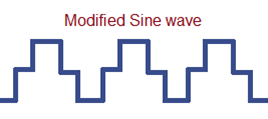
In the previous tutorial, square wave inverter was designed. Square wave inverter was simple to design but had certain drawbacks. The AC appliances are actually designed to operate on sine wave and square wave though being AC signal does not match to an ideal sine wave.Due to this, when an appliance is powered by a square wave inverter, it may have noise or humming sound during its operation. So, designing of a modified sine wave inverter will be discussed in this tutorial.