Nowadays most of the electronic devices are portable and they run ob batteries. Batteries store charge temporarily and discharge by supplying power to the attached device. While one problem with the use of batteries is overcharging, another common problem is over discharging. In this project, a circuit is designed which will keep track of the charge level of the attached battery and it will automatically switch the supply source to the load circuit from the battery to the DC source.
Also when the battery will reach its end of discharge voltage, it will start charging the battery and when the battery will be fully charged or reaches to its maximum rated terminal voltage, it will again switch the supply source to the load circuit from DC to the battery. The end of discharge voltage is the voltage below which battery may die prematurely and degrades its recharge capabilities. Any battery should be charged before its charge level drops to end of discharge level.
In this experiment, a 12V lead acid battery is taken. The end of discharge voltage of 12V lead acid battery varies among the manufacturers. In this experiment, the battery used has an end of discharge voltage of 11V and its maximum rated terminal voltage is 13.8 V. During the project development, it was observed that when the battery reached to 11.04 V then the load circuit automatically connected to the DC source and so the battery was saved from deep discharge. When the battery was fully charged to 13.9 V then again the load connected to the battery.
In this series, already an automatic overcharging battery cut-off circuit and an automatic over discharging battery cut off circuit has been designed. However, it is not possible to combine those circuits together to automatic cut off the battery for both cases when the battery over discharge and overcharge as well. In this project, a feature to automatically charge the battery when the battery is discharged and again switch the battery to load when it is fully charged is desired.
Previously, for overcharge protection and over discharge protection, a circuit as shown below was used –

Fig. 1: Circuit Diagram of Battery Protection from Over Charging
In this circuit when the battery will go below its end of discharge voltage i.e. approximately 10.7 V, then the relay will activate. Now the load will disconnect from the battery and battery will start charging. During charging when the battery voltage is slightly increased from its end of discharge voltage then the relay will deactivate and the battery will connect to the load before the battery is fully charged.
To avoid this problem, some latching circuit has to be used which enables or activates the relay when the battery is discharged and deactivates the relay only when the battery is fully charged. So, building upon the same circuit as in the previous projects, a latching circuit is added in this project.
Components Required

Fig. 2: List of Components required for Automatic Power Supply Switching For Battery Operated Devices
Circuit Connections –
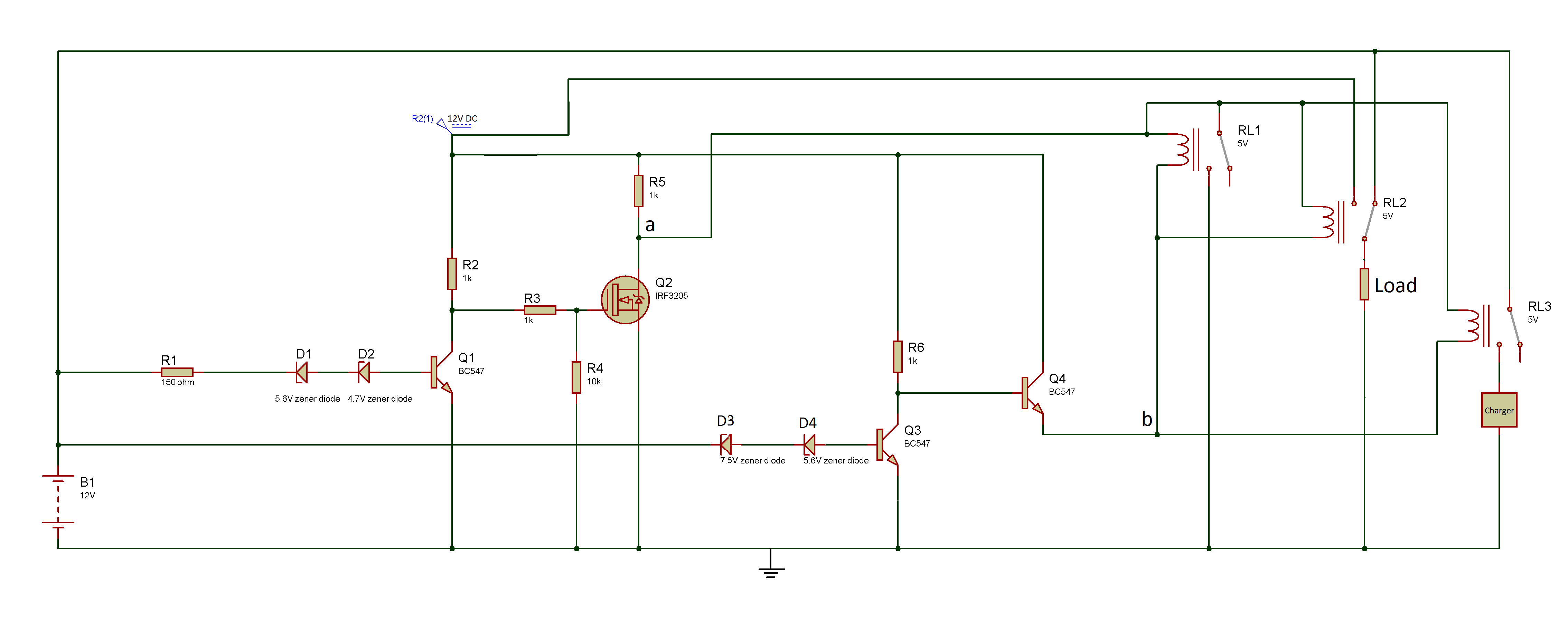
In this switching circuit, the source of power supply to a load circuit is changed between the battery and DC power. The main components that play important role in the functioning of this circuit are the relay, switching transistors and zener diode.
Relay as a latch and switching circuit
In this circuit, there are three relays used. The first relay (shown as RL1 in the circuit diagram) is the key of this circuit. As already mentioned some latching circuit is must for this project, so the relay RL1 act as a latch in this circuit. This latching circuit activates the relay RL2 and RL3 when the battery goes below the end of discharge voltage. Both the relay RL2 and RL3 deactivates only when the battery is fully charged. In the circuit relay, RL2 is used for switching the load to DC source or the battery. The relay RL3 is used for connecting the battery to the charger when the battery gets below the discharge voltage and again disconnect the battery from the charger when the battery is fully charged. So the use of multiple relays confirms to the use of latching as per the circuit requirements.
Switching Transistor for activating and deactivating the relay
The transistor circuit is used to operate the relay. The transistors are used as high side switch where the transistor stages are operating as logical inverters. A relay will activate when its energizing ends will get sufficient potential difference to activate the relay. When a potential difference of energizing pins is equal or greater than the relay rating then only it gets activated. In this experiment, the one energizing pin of all the three relays (RL1, RL2, RL3) are connected to the collector of transistor Q2. Whenever Q2 is in ON state then all the current from its collector drains to the ground. So, in this state, the collector of transistor Q2 will provide ground to the one end of the relays.
Another energizing pin of all the relays is connected with the emitter of transistor Q4. Now this circuit, the transistor Q4 provides some potential to the another end of relays for activation of the relays. Whenever transistor Q4 will be ON then all the current from its collector will flow to its emitter and this emitter will then provide the voltage to energizing ends of all the relays.
Hence when both the transistor Q2 and Q4 will be ON, then all the relays will activate, otherwise, they will remain in the non-active state. The transistors Q1 and Q3 control the base voltage of transistors Q2 and Q4 respectively.
Zener diode for sensing the end of discharge and maximum battery voltage
A zener diode is connected in series with the battery such that the cathode of the zener diode is connected with the anode of the battery and anode of the zener diode is connected with the base of the switching transistor. The purpose of connecting the diode in this manner is to operate it in reverse biased condition. When a zener diode is connected in reverse bias configuration and its cathode voltage is below its breakdown voltage then the zener acts like an open circuit. But when a voltage above zener breakdown is applied at its cathode terminal then zener starts conducting from the cathode to anode while Zener is in reverse bias condition. As the zener diode can also work in reverse bias condition, this feature of the zener diode is utilized for detecting the cutoff voltage level of the battery. In this circuit, zener diode is used to detect the end of discharge voltage and maximum rated voltage of the battery.
The battery used in this experiment has the end of discharge voltage of 11 V and the maximum rated voltage of 13.8 V. So, the circuit is designed such that it disconnects the battery from the load when the battery reaches at 11 V and again connects the battery to the load when the terminal voltage of the battery is 14 V. So, there are two zener diodes used in the circuit one with peak inverse voltage of 11V and another zener having peak inverse voltage of 14 V.
The 11V zener diode is connected in reverse bias with the transistor Q1 and 13.8 V zener diode is connected with the transistor Q3 (as shown in the circuit diagram). Therefore, whenever the terminal voltage of the battery drops down to 11V then 11V zener diode does not conduct and transistor Q1 goes in the OFF state. When the battery voltage exceeds 13.8 V then 13.8 V zener diode starts conducting and transistor Q3 goes in ON state. So, by detecting both the transistors Q1 and Q3 ON and OFF state, the end of discharge and maximum voltage of the battery are detected.
For selecting the zener diode, the threshold voltage of the switching transistor used i.e. BC547 in this circuit has to be considered which is connected in series with the zener diode.
For selecting Zener diode for battery end of discharge voltage –
(Zener voltage) Vz = 11V – (threshold voltage of the transistor BC547 )
(Zener voltage) Vz = 11 – 0.7 = 10.3 V
For Selecting Zener diode for maximum voltage of the battery –
(zener voltage) Vz = 13.8V – (threshold voltage of the transistor BC547 )
(zener voltage)Vz = 13.8 – 0.7 = 13.1 V
So, two zener diodes D1 (5.6V) and D2 (4.7 V) have been taken to make a total of 10.3 V for detecting battery end of discharge voltage. Two zener diodes D3 (7.5V) and D4 (5.6V) are taken to make a total of 13.1V for detecting the maximum voltage of the battery.
How the circuit works –
The circuit is based on the working of zener diode. A zener diode when connected in reverse bias configuration and its cathode voltage is below its breakdown voltage then zener acts like an open circuit. But when a voltage above zener breakdown is applied at its cathode terminal then zener starts conducting from the cathode to anode in reverse bias condition. The zener diodes drive the transistor stages which control the state of the relays. For understanding the operation of this circuit consider different battery voltage levels as follow –
Case 1: When battery voltage is at 12V
As the total breakdown voltage of zener diodes D3 and D4 is 13.1 V, so in this state the zener diode does not conduct. The transistor Q3 will be in off state so the base of the transistor Q4 will get positive voltage to turn ON. Hence all the current from Q4 collector goes to its emitter and at point ‘b’ the relay end will get some positive voltage.
The total breakdown voltage of zener diodes D1 and D2 is 10.3V, so in this state the zener diode is in reverse biased condition and start conducting from its cathode to anode terminal. This makes the transistor Q1 ON. Due to conduction of transistor Q1, the base of the transistor Q2 is grounded and Q2 goes in off state. So, at point ‘a’ the relay end will not get ground and it will remain in non-active state. As all the relays are not active so the battery remains connected to the load circuit and that is what desired for this battery voltage.

Fig. 3: Circuit Diagram showing operation of Automatic supply switching for battery voltage at 12V
Case 2: When battery voltage drops down to 11V (end of discharge voltage of battery)
When the battery starts discharging and its voltage is dropped down to 11V then zener diodes D1 and D2 will stop conducting. Now transistor Q1 will turn off and base of the transistor Q2 gets the positive voltage to conduct. The conduction of transistor Q2 drains all the current from its collector to ground and at point ‘a’ zero voltage difference is obtained. This provides ground to the relay energizing pin. Again in this state, the zener diodes D3 and D4 does not conduct.
The transistor Q3 will be in off state so the base of the transistor Q4 will get positive voltage to turn ON. Hence all the current from collector of transistor Q4 goes to its emitter and at point ‘b’ the relay end will get some positive voltage. Now the relay will get sufficient voltage at its both energizing pins and all the three relay will get activated. The load will switch from battery to DC source through relay RL2. The battery will connect with the charger by relay RL3 and starts charging.

Fig. 4: Circuit Diagram showing operation of Automatic supply switching for battery voltage at 11V
Case 3: When battery voltage exceeds to 11V but less than 13.8 V
When the battery starts charging and it exceeds its end of discharge voltage (11V) but not get fully charged, the zener diodes D1 and D2 will again start conducting and turn ON the transistor Q1. This will ground the base of transistor Q2. Then transistor Q2 will be off so all the relay should get deactivated. But because the relay RL1 is used as a latch so the NO (normally open) pin of the relay RL1 is permanently connected to the ground. Further relay common pin is directly connected with the energizing pin of the RL1 and Common pin is also connected to the NO pin of relay RL1 in the active state. So, the relay if once get activated then remain in active state as its energizing pin will get continuous ground from its common pin. Due to this, the relay will get ground reference spite of what the voltage at point ‘a’ is.

Fig. 5: Circuit Diagram showing Relay Operation
In this case, zener diodes D3 and D4 will not conduct. So, another end of energizing pin of relay remains at high voltage due to conduction of transistor Q4 and non-conduction of transistor Q3. Therefore, all the three relays will be in active state and the battery will remain connected with charger and the load with the DC source.

Fig. 6: Circuit Diagram showing operation of Automatic supply switching for battery voltage between 11V and 13.8V
Case 4: When battery voltage exceeds to 13.8 V (battery is fully charged)
When the battery is fully charged, and reaches its maximum rated voltage of 13.8 V then in this case, the transistors Q1 and Q2 will remain in its previous state. But the zener diodes D3 and D4 will breakdown and start conducting. The transistor Q3 will be ON and this grounds the base of transistor Q4. So the transistor Q4 will not remain in conducting state and there will be no more current which flows from collector of transistor Q4 to its emitter. So, at point ‘b’ the relay will no more get any positive voltage at its energizing pin. Thus, all the relays will get deactivated. The load then again switches from DC to the battery and the battery will disconnect from the charger.

Fig. 7: Circuit Diagram showing operation of Automatic supply switching for battery voltage at 13.8V
Use of series resistance (R1) with zener diode and with other components
A zener diode requires a series resistance which limits the flow of current through it above its current rating, this will prevent the zener from overheating. With the use of series resistance, zener can provide a regulated voltage at the output. The resistances used at the collector and base of all the transistors are just to limit the current on their base and collector so that they do not blow off due to high current. The resistance R4 at the base of transistor Q2 acts as a pull-down resistor. As FET start conducting for very small value of current at its base, so resistance R4 is used, so that transistor Q2 does not get ON by any unwanted external noise.
Selection of Zener Diode Series Resistance (R1)
In this experiment the zener diode used has 10.3 V/250 mW rating. The series resistance of zener can be calculated by the following equation-
R1 = (Vs-Vz)/Iz
Where,
Vs = maximum supply voltage
Vz = zener voltage
Iz = zener current
For calculating R1 the Zener current needs to be calculated as follows –
Maximum Power dissipation of zener diode, Pz = 250mV
Zener voltage, Vz = 5.6+4.7= 10.3V
Total voltage for which zener should start conducting, V1 (Vz + typical threshold voltage of BC547 Q1 transistor)
V1 = 10.3+0.7
V1 = 11V
So, maximum zener current, Iz can be calculated as follows –
Pz = V1 * Iz
Iz = Pz / V1
Iz = 0.25/11V
Iz = 22mA (approx.)
As the 12V lead acid battery charge upto 13.8 V, so the maximum supply voltage from the battery, Vs = 13.8 V
Zener voltage, Vs = 13.8V
Now using the above values, resistance R1 can be calculated as follows –
R1 = (Vs-Vz)/Iz
R1 = (13.8-11)/0.022
R1 = 127 ohms(approx)
In the experiment, for convenience the resistance R1 is taken 150 ohms which is round off value.
There is no resistance used with D3 and D4 zener diodes as the battery voltage will never exceed higher than the 13.8 V. It is important that the selection of zener series resistance must be done wisely. It should not allow current more than the zener rating, as more current will permanently damage the zener diode.
Theoretical cut off voltage for battery overcharge and over discharge states
Battery over discharge cut-off voltage, Voverdis= (Vz + typical threshold voltage of BC547 transistor)
Voverdis= 10.3 + 0.7 = 11V
Battery over dischargecut-off voltage, Vovercharge=(Vz + typical threshold voltage of BC547 transistor)
Voverdis= 13.1 + 0.7 = 13.8V
The DC source voltage should be greater than the relay voltage rating otherwise the relay will never energize. In this experiment, the DC source is of 12V and as transistor Q4 will supply the voltage to the relay energizing pin so relay will not get exact 12V (due to resistive losses) at its pin so never get active. Due to this fact, a 5V relay is used. Also do not charge the battery with a constant voltage charger as in constant voltage charger a direct voltage of maximum battery rating is applied to the battery. So, during charging the battery voltage will be at its maximum rated voltage of the battery which will give an indication to the circuit that the battery is fully charged. Therefore, charge the battery only with a constant current charger.
Testing –
When a 12 V battery is connected and the battery voltage drops down to 11.04 V then battery get disconnected from the load. This can be determined as follows –
(Practically)Voverdis=(Vz + typical threshold voltage of BC547 transistor or Vbe )
(Practically)Voverdis=10.3 + 0.74
(Practically)Voverdis= 11.04V
When the battery voltage is at 13.9 V then the battery will again connect to the load. This can be determined as follows – (Practically)Overcharge= Vz + typical threshold voltage of BC547 transistor or Vbe )
(Practically)Vovercharge = 13.1 + 0.8
(Practically)Vovercharge =13.9V
So, the circuit will cut off the battery from the load when the battery voltage goes below 11.04 V and again connect the load to the battery when battery voltage goes above 13.9 V.

Fig. 8: Prototype of Automatic Supply Switching Circuit for Battery Protection on Breadboard
This circuit can be easily modified for any another battery pack by just changing the zener diode values. There will be automatic switching of load from battery to DC when battery reaches to end of discharge voltage and there will be automatic charging of the battery and the battery will again connect to the load when the battery will be fully charged.
From the circuit diagram, it can be noted that MOSFET is used in place of BJT for transistor Q2. As the transistor Q2 collector will provide the ground to the relay energizing pins. So if there would have been used a BJT then in the ON state of transistor Q2, the relay will get almost zero volts from the collector of Q2 and the relay would have never got activated.
This would have also caused the voltage at the collector to emitter of transistor Q2 to be exact zero volts, since relay NO pin is directly connected to the ground. But in ON state of BC547 transistor (Q2), the Vce is 0.2V. So, the exact zero volts could disrupt the biasing of transistor Q2. That is why, the MOSFET is used in place of BJT as MOSFET ON and OFF state will not depend on the voltages at the drain and source. It only depends on the gate voltage. Thus, the biasing of MOSFET does not disrupt when the relay activates.
Circuit Diagrams
Filed Under: Electronic Projects

Questions related to this article?
👉Ask and discuss on Electro-Tech-Online.com and EDAboard.com forums.
Tell Us What You Think!!
You must be logged in to post a comment.