The communication technology had its debut with wired communication. The wired communication is still popular and used wide-spread for telephony and internet. Though it was soon realized that wired communication has its own limitations. Its installation incurs high cost and the installation becomes more complicated as the system grows. Moreover wired communication was never a suitable medium for many consumer electronics, industrial and military applications. Then, the discovery of electromagnetic waves and their application in communication came as a great advancement for the mankind.
The world was first introduced to wireless communication when Guglielmo Marconi developed first wireless telegraph system in 1896. The technology progressed in early 1900s with the introduction of commercial radiotelephony and by 1960s first communication satellites were in space. Another decade saw the introduction of cellular systems and mobile communication sought to became a norm by late 1980s in the developed countries. Till this time, use of radio communication for mobile telephony, television broadcasting and satellite and radio based communication for military applications had gained full momentum.
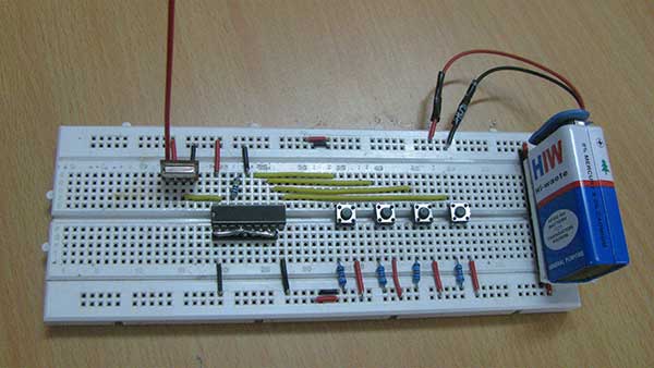
Fig. 1: Prototype of RF Transmitter
From 1990s onwards wireless communication found a different dimension apart from its use in telecommunication, military and space applications. This was the use of low-band radio frequency communication for data transfer to smaller distances. The telecommunication sector utilized this by introducing the technologies like Bluetooth for transferring data from one device to another over few meters and Wi-Fi for routing internet wireless in a home or office environment. The consumer electronics sector also utilized these standard wireless communication technologies and additionally utilized other low band radio frequency technologies for equipping their appliances with remote control and wireless data transfer.
The performance of any wireless system is judged based on two parameters – distance it can transfer data and the rate (data rate) at which it can transmit and receive data. The wireless systems use a wide range of frequencies from 30 KHz to 300 GHz. The higher the frequency higher is the distance of operation. For small distance communication, low band frequencies of few KHz or MHz are used.
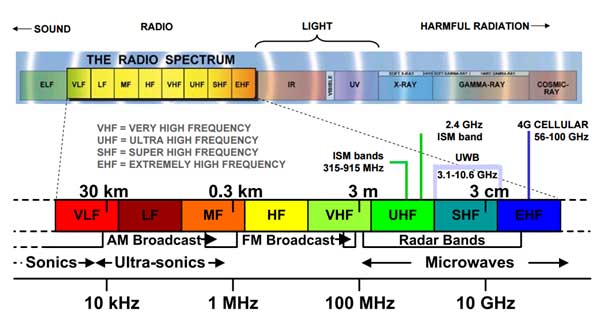
Fig. 2: Diagram of Radio Spectrum
The following project is also a demonstration of low-band radio frequency communication using a 434MHz RF module. These kinds of radio communication modules have distinct advantages over other remote control technologies like the infrared. These modules do not need a line of sight for operation and they can be used over a wide array of operating voltages ranging from 3V to 12V.
How Radio Frequency Communication Works
Like any communication system, RF systems also have a transmitter end which transmits electromagnetic waves with data encoded in them and a receiver end which receives these waves and retrieve data from them.
Several carrier frequencies are commonly used in commercially-available RF modules, including those in the industrial, scientific and medical (ISM) radio bands such as 433.92 MHz, 915 MHz, and 2400 MHz the selection of 434MHz among these frequencies is because of national and international regulations governing the use of radio frequency for communication. Short Range Devices can also use frequencies such as 315 MHz and 868 MHz available for unlicensed use.
At the transmitter end, the electromagnetic waves need to be modulated for encoding data in them. Here modulation means that one of the characteristic of the wave like amplitude, frequency or sequence is changed according to the digital data that has to be transferred. There are a myriad of modulation techniques like ASK, OOK, FSK, Direct sequence spread spectrum, Frequency hopping spread spectrum and GFSK which are used by radio communication systems for representing data. The selection of the modulation technique depends on the application and requirements. The modulation technique used in this 434 MHz RF module is ASK (Amplitude Shift Keying) which is the most commonly used modulation technique in low band radio communications.
At the receiver end, a reverse process called demodulation using the same demodulation technique (ASK in this case) is carried out and the data is extracted from the carrier wave.
One important aspect of working with RF modules is the identification of transmitter and receiver with respect to each other. This is called pairing. It is done by matching an identification key set at both ends. The data is serially transmitted and received. Thus data from a microcontroller or processor may need to be serialized using an encoder and at the receiver end it may need to be decoded using a decoder for parallel data transfer. The encoder and decoder ICs used in this module are HT12E and HT12D respectively.
Components Required
| COMPONENTS | NUMBER |
|---|---|
| RF Transmitter and receiver module ( 434 MHz) | 1 |
| HT12E/HT12D Encoder IC | 1 |
| LED | 1 |
| Resistor – 10KΩ (Quarter watt) | 8 |
| Resister-1MΩ (Quarter watt) | 1 |
| Battery-9V | 2 |
| Connecting Wires | |
| Breadboard | 2 |
BLOCK DIAGRAM

Fig. 3: Block Diagram of RF Transmitter and Receiver
Working of Circuit
Circuit Connections
As seen from the block diagram, the RF circuit comprises of two sections – :
1) Transmitter section – This section comprises of a HT12E encoder chip, RF transmitter and Antenna are shown below – :
a) HT12E Encoder – The HT12E IC converts the parallel data into serial data for passing it to the RF transmitter. HT12E encoder IC belongs to the 212 series of encoders. It is paired with 212 series of decoders having the same number of addresses and data format. These ICs are mainly used for interfacing RF and infrared circuits. HT12E is capable of encoding 12 bits, out of them 8 are address bits and 4 are data bits. Thus the encoded signal is a serialized 12-bit parallel data comprising of 4-bit data to be transferred appended with the address byte. The pin diagram and configuration of HT12E are shown below – :
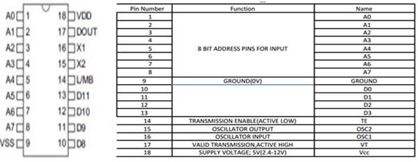
Fig. 4: Pin Diagram and Pin Configuration of HT12E RF Encoder IC
b) RF Transmitter – The RF transmitter consists of an electrical oscillating circuit which generates the radio wave, a modulator which perform hybrid ASK modulation of the wave according to the digital data received from the encoder, and an amplifier which increases the strength of modulated signal for transmission.
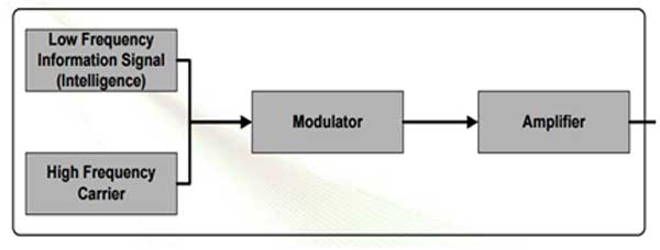
Fig. 5: Block Diagram of RF Transmitter
The RF transmitter module is a small PCB sub assembly. The pin configuration of transmitter module is as follow – :
| PIN NO. | FUNCTION | NAME |
|---|---|---|
| 1 | Ground(0V) | Ground |
| 2 | Serial data input pin | Data |
| 3 | Supply Voltage ; 5V | VCC |
| 4 | Antenna output pin | ANT |
The serialized data from encoder is received at pin 2 of the module and passed on to the antenna from pin 4 of the module.
Finally, the modulated signal is transmitted through the antenna
2) Receiver section – This section comprises of Antenna, RF receiver and HT12D decoder chip. The modulated RF signal is received by the antenna and passed to the RF receiver.
a) RF Receiver – The RF receiver consists of an amplifier that amplifies the received signal, a demodulator or detector which extracts the modulated signal from the carrier wave, a modulated signal amplifier and an output transducer.
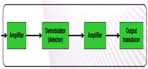
Fig. 6: Block Diagram of RF Receiver
There are two types of RF receivers – Super heterodyne receiver and super regenerative receiver. The receiver module has 8 pins and has following pin configuration.
| PIN NO. | FUNCTION | NAME |
|---|---|---|
| 1 | Ground(0V) | Ground |
| 2 | Serial Data output pin |
Data |
| 3 | Linear output pin ; not connected | NC |
| 4 | Supply voltage ; 5V | VCC |
| 5 | Supply Voltage ; 5V | VCC |
| 6 | Ground(0V) | Ground |
| 7 | Ground(0V) | Ground |
| 8 | Antenna input pin | ANT |
The carrier wave from the antenna is received at the pin 8 of the module. The extracted data in serial form is output at pin 2 of the module.
b) HT12D Decoder – The signal extracted from the RF receiver is passed to the HT12D decoder. It converts the serial data back to the parallel data after separating data and addresses. HT12D belongs to the 212 series of decoders and can be paired with 212 series of encoders having the same number of addresses and data format. HT12D is capable of decoding 12 bits, out of them 8 are address bits and 4 are data bits. The 4-bit data is of latch type and when passed to the output data pins it remains unchanged until the new data is received.
The pin diagram and configuration of HT12D is as follows – :

Fig. 7: Pin Diagram and pin configuration of HT12D RF Decoder IC
How the Circuit Works
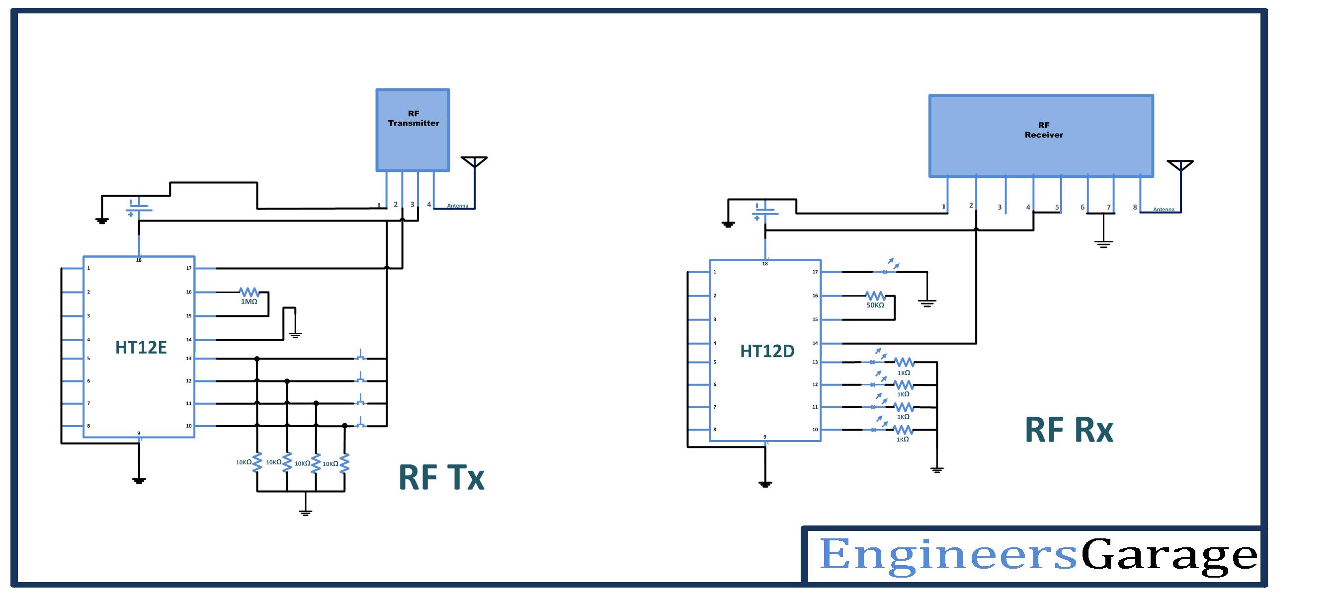
The data in this RF module is transmitted as 4-bit data. The data to be transferred is hard-wired with the help of switches at pins 10 to 13 of the HT12E IC designated as D0 to D3 respectively according to the pin configuration of the IC. Here 10K ohm resistors are used at data pins as pull-up resistors. The address of the transmitter is also hard-wired. Here all address pins are grounded to allot transmitter an address of 0x00. The pin 14 of the IC is grounded to enable transmission as it is active LOW. A switch can also be connected to pin 14 of the IC to reset transmission. To set the oscillator, a resistor from 750MΩ to 1MΩ can be connected between pin 15 and 16 of the encoder IC. Here a 1MΩ resistor is used in the circuit. The serialized data is passed on from pin 17 of the encoder IC to the pin 2 of the RF transmitter. A modulated carrier wave is output from pin 4 of the RF transmitter and transmitted through the antenna.
At the receiver end, the modulated carrier wave is detected by the receiver antenna and passed on to pin 8 of the RF receiver. The demodulated signal is output from pin 2 of the RF receiver which is sent to pin 14 of HT12D decoder IC for converting to parallel data from the serial form. A resistor between 30KΩ to 50KΩ can be connected between pins 15 and 16 of the decoder IC to match the oscillator settings. Here, a 50KΩ resistor is used in the circuit. These values of the resistances are dictated as according to the datasheets of HT12E and HT12D ICs. The address at the decoder IC is again hard wired and should match with the address at encoder IC to enable the pairing of transmitter and receiver.
Here all address pins are grounded to match the 0x00 address at the transmitter end. The received data is fetched at pins 10 to 13 of HT12D which are designated as D0 to D3 respectively according to the pin configuration of the decoder IC. In the experiment, received data is detected with the help of LEDs. An LED serially connected to a 1KΩ pull-up resistor is interfaced to each data pin to detect the digital signal at the respective pin. If the LED glows that means a HIGH signal is receiving at that pin else a LOW signal is receiving at that pin. As the data is changed at the encoder IC on altering the on/off status of the switches at data pins of the encoder IC, a similar change in the on/off status of the LEDs connected to data pins of the decoder IC is reflected.
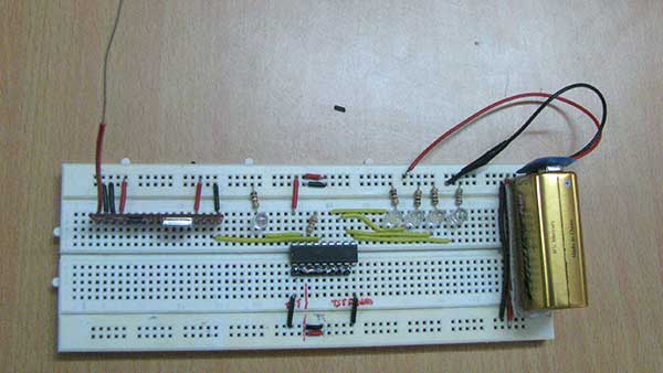
Fig. 8: Prototype of RF Receiver
This experiment is a simple demonstration of RF transmission using HT12E/HT12D ICs and RF modules. A single pair of RF transmitter and receiver modules is paired in the experiment. However, any number of receivers can be configured to receive data from a single transmitter module or even any number of transmitters can be configured to transmit data to a single receiver. The only important thing is that the addresses at the encoder of transmitter and decoder of receiver modules should match. A complex system of RF data network can be formed by enabling the alteration of the addresses of transmitter and receiver modules.
In the experiment data pins are hard-wired by connecting to switches at transmitter end and LEDs at the receiver end but they can be connected to microcontrollers or other logical circuits to make use of RF transmission in some real-life application. Some possible application of RF transmission can be remote-controlling a robot or a group of robots, Contact-less RF smartcard or radio tags reading, wireless data acquisition from a remotely installed sensor, remote message transmission to a display device, area paging, wireless home automation using multiple receivers connected to home appliances and a single remote having a RF transmitter, telemetry, Access Control System (Like remote controlled garage door) etc.
Circuit Diagrams
Filed Under: Electronic Projects


Questions related to this article?
👉Ask and discuss on EDAboard.com and Electro-Tech-Online.com forums.
Tell Us What You Think!!
You must be logged in to post a comment.