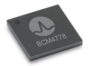
Broadcom Inc. recently announced the world’s lowest power L1/L5 GNSS receiver chip: the BCM4778. Optimized for mobile and wearable applications and equipped with the latest GNSS innovations, this third-generation chip is 35 percent smaller and consumes five times less power than the previous generation.
 Dual-frequency GNSS continues to be an important location feature for modern mobile and wearable devices as it provides greater positioning accuracy for location-based services (LBS) applications. The advanced L5 signal enables sidewalk-level accuracy for pedestrian navigation in urban environments, as well as lane-level accuracy for vehicle navigation.
Reduction in GNSS power consumption is crucial to extending the battery life of a mobile or wearable device. Compared to GNSS receivers used in integrated platforms, Broadcom’s single-chip BCM4778 delivers significantly lower power consumption and higher performance while offering more advanced GNSS features — such as the next-generation Grid Tracking urban multi-path mitigation technology.
Additionally, the BCM4778 increases the GNSS always-on battery lifetime on a smartwatch by 30 hours compared to the previous generation chip operating on a 300mAh battery. The extended battery life benefit helps drive new experiences in smart watches and phones.
For example, smart watches can keep the GNSS always-on for fitness applications for multiple days on a single battery charge. Also, the BCM4778 features fully integrated LNAs for L1 and L5 bands, which reduces RF front-end BOM costs and footprint requirements, which is ideal for space-constrained applications.
The chip offers immense flexibility to smartwatch and phone designers with its small size. Having the ability to place the BCM4778 closer to the antenna helps improve signal reception and thereby enhance the overall GNSS performance.
“Consumer electronic companies have been faced with the challenge of managing power consumption versus performance, often having to choose one over the other. Broadcom’s innovative approach to the BCM4778 allows their customers to realize improvements on both fronts,” said Ramon T. Llamas, research director for mobile devices at IDC. “The result: device manufacturers can enable new experiences and run applications over a sustained period of time. In addition, by reducing its BOM cost and its physical footprint, Broadcom is enabling further benefits from cost savings and design configurability.”
Highlights
- 7nm CMOS technology
- Typical power consumption
- 4mW L1 band only
- 6mW L1+L5 simultaneous
- FCBGA package
- New Grid Tracking™ technology
- Advanced multipath mitigation
- Continuously tracks the full L5 channel
- Capable of L5 acquisition
- Increased processing capability and throughput
- Advanced LTE filtering and jamming mitigation
- Enhanced LTE Band 13 and Band 14 filtering
- Spoofing and jamming detector
- Jamming mitigation through multiband and multi constellation
- Reduced BOM cost and footprint
- Flexibility in using internal LNAs
- Optional operation without interstage SAW filters
- Integrated switching regulator with direct connect to battery
“With the launch of this third-generation, dual-frequency GNSS receiver chip, Broadcom continues the tradition of raising the bar for mobile GNSS,” said Vijay Nagarajan, VP of marketing for the Wireless Communications and Connectivity Division at Broadcom. “Always-on dual frequency GNSS is a key request from mobile and wearable OEMs, and we are thrilled to deliver it.”
Filed Under: Components, News, Smart Wearables


Questions related to this article?
👉Ask and discuss on Electro-Tech-Online.com and EDAboard.com forums.
Tell Us What You Think!!
You must be logged in to post a comment.