In the first tutorial of this series – Introduction to Digital Electronics, it was mentioned that there are different code systems that are used to represent digital information as binary numbers. Each code system has different binary numbers assigned to same symbols and characters. The different digital systems may be using different code systems. In such case, there must remain some code conversion circuit to make the interconnected digital systems compatible.
In this tutorial, code conversion circuits will be designed using SN7400 series of digital ICs. In the previous tutorial, the same series of digital ICs was used to construct arithmetic circuits like half adder, full adder, half subtractor and full subtractor. In this tutorial, the following code conversion circuits will be designed –
· Binary to Gray code converter
· Gray to binary code converter
· BCD to excess – 3 code converter
· Excess – 3 to BCD code converter
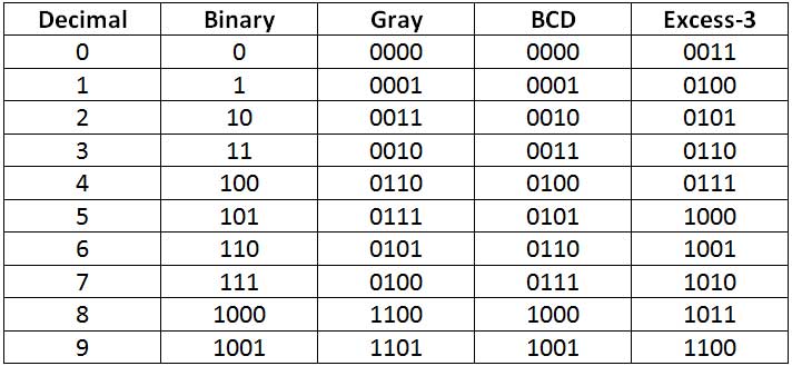
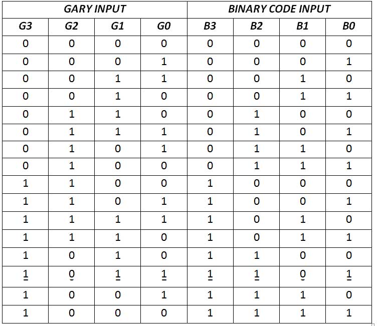
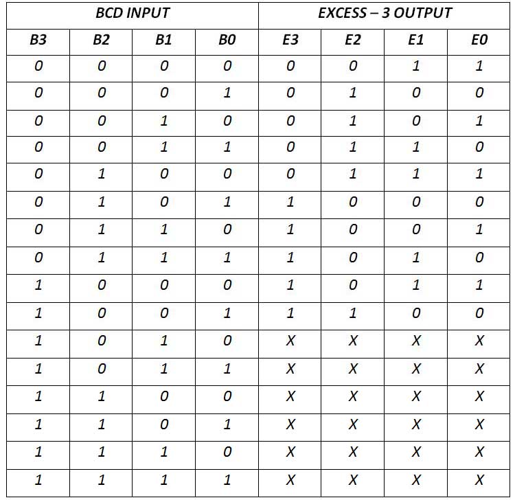
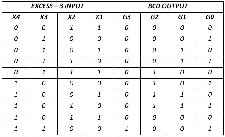
The code conversion circuits designed in this tutorial will be used for conversion of digits 0 to 9 from one code system to another. The different code systems have different binary numbers assigned to the digits. Like in gray code, the binary numbers are ordered in such way that any two successive digits or values differ only by one bit. The BCD numbering system is similar to binary representation of the decimal numbers except that the coded number is separated into four bits for each digit in the decimal number. So, the coded number is represented by weighted binary values where each value is 4-bit long and direct representation of the digits in the decimal number. The Excess-3 code is similar to BCD numbering system with only difference that each 4-bit long value in the coded number is obtained by adding 3 to the BCD representation. The following table summarizes the binary representation of digits 0 to 9 in different code systems –
With the knowledge of these code systems, Let us now start building the code converter circuits.
Components Required –
Circuit Diagrams –
The Binary to Gray Code Converter has the following circuit diagram –
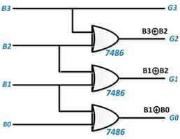
Fig. 1: Binary to Gray Code Converter Combinational Circuit
The Gray to Binary Code Converter has the following circuit diagram –
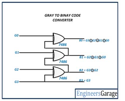
Fig. 2: Gray to Binary Code Converter Combinational Circuit
The BCD to Excess – 3 Code Converter has the following circuit diagram –
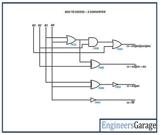
Fig. 3: BCD to Excess-3 Code Converter Combinational Circuit
The Excess – 3 to BCD Code Converter has the following circuit diagram –
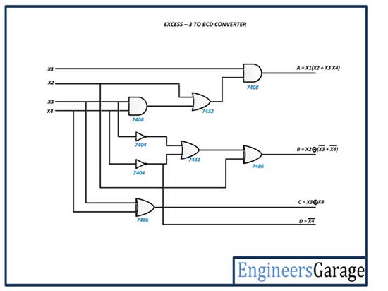
Fig. 4: Excess-3 Code to BCD Converter Combinational Circuit
Circuit Connections –
The code converter circuits designed in this tutorial are combinational circuits as their output is dependant only on the present input values. Each circuit has a unique truth table from which the respective boolean expression for each output can be derived. The minimized boolean expression is then converted into logic gate diagram which is built on a breadboard using 7400 series ICs.
The following logic gate ICs are used in the construction of the circuits –
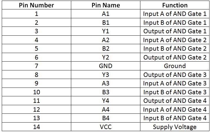
7408 IC – The 7408 IC has quad 2-input AND gates. The IC has the following pin configuration –
The IC has the following Pin Diagram –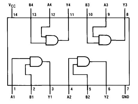
Fig. 5: 7408 Pin Diagram
The IC requires a supply voltage of 5V which can be tolerated up to 7V. The voltage at the inputs of AND gates must be 2V for high logic and 0V for low logic. The output of the AND gates has a voltage of 3.4 V for high logic and 0.2 V for low logic. The IC operates on positive logic system. The propagation delay while transiting from LOW to HIGH level at the output is 27 ns while propagation delay while transiting from HIGH to LOW level at the output is 19 ns.
7432 IC – The 7432 IC has quad 2-input OR gates. The IC has the following pin configuration –
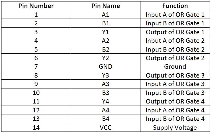
The IC has the following Pin Diagram –
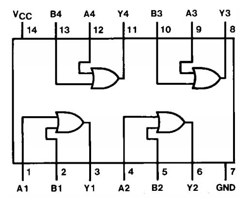
Fig. 6: 7432 Pin Diagram
The IC requires a supply voltage of 5V which can be tolerated up to 7V. The voltage at the inputs of OR gates must be 2V for high logic and 0V for low logic. The output of the OR gates has a voltage of 3.4 V for high logic and 0.35 V for low logic. The IC operates on positive logic system. The propagation delay while transiting from LOW to HIGH level at the output comes 3 to 15 ns while propagation delay while transiting from HIGH to LOW level at the output also comes 3 to 15 ns.
7486 IC – The 7486 IC has quad 2-input EX-OR gates. The IC has the following pin configuration –
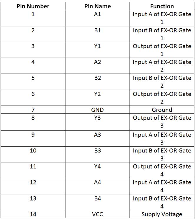
The IC has the following Pin Diagram –
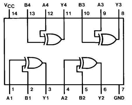
Fig. 7: 7486 Pin Diagram
The IC requires a supply voltage of 5V which can be tolerated up to 7V. The voltage at the inputs of EX-OR gates must be 2V for high logic and 0V for low logic. The output of the EX-OR gates has a voltage of 3.4 V for high logic and 0.2 V for low logic. The IC operates on positive logic system. The propagation delay while transiting from LOW to HIGH level at the output is 23 ns if other inputs are low and 30 ns if other inputs are high while propagation delay while transiting from HIGH to LOW level at the output is 17 ns if other inputs are low and 22 ns if other inputs are high.
7404 IC – The 7404 IC has six inverting gates. The IC has the following pin configuration –
The IC has the following Pin Diagram –
Fig. 8: 7404 Pin Diagram
The IC requires a supply voltage of 5V which can be tolerated up to 7V. The voltage at the inputs of NOT gates must be 2V for high logic and 0.8 V for low logic. The output of the NOT gates have a voltage of 3.4 V for high logic and 0.2 V for low logic. The IC operates on positive logic system. The propagation delay while transiting from LOW to HIGH level at the output is 22 ns while propagation delay while transiting from HIGH to LOW level at the output is 15 ns.
It must be noted that the selected ICs have compatible input, output and supply voltage levels as they are taken from a common family (74XX series) of digital ICs.
How the circuit works –
There are different code systems available for representation of digital information. Many times, the digital systems use components that might be using different code systems. In such case, there must be some code converter circuit between such components, so that they could communicate digital information between them. The commonly used code systems include Gray code, BCD and Excess-3. In all these code systems, each binary digit is represented by a unique 4-bit value. For convenience, the binary input in binary to gray code converter and binary output in gray to binary code converter is also taken 4-bit long.
So as each code uses four bits to represent a decimal digit, there are four inputs and four outputs. It must be noted that Gray code is a non-weighted code while BCD and Excess-3 are weighted code systems. In BCD and Excess-3 code converters, the circuit is designed only for conversion of single digit. The input variable are designated as B3, B2, B1, B0 and the output variables are designated as G3, G2, G1, G0. From the truth table, the K-maps for each of the four outputs of the respective circuits are obtained and boolean functions involving four input variables for each output variable are derived. A two-level logic diagram is obtained directly from the Boolean expressions derived by the maps and combinational circuits are designed for each variable in the respective circuits.
Binary to Gray Code Converter –
The binary numbers are non-weighted representation of decimal numbers in base 2. The gray code which is also called Reflected Binary Code (RBC) or just Reflected Binary (RB) has binary numbers ordered for the decimal digits in such way that any two successive values differ only by one bit. The gray code is widely used in digital communication systems for error correction. The input binary numbers here are assumed to be 4-bit long. For deriving gray code equivalent of the binary numbers, first the MSB (Most Significant Bit) is written down as it is then each lower place digit in gray code number is obtained by adding the respective bit and the bit one place lower in the binary number. The circuit has four inputs (B3 B2 B1 B0) representing 4-bit binary numbers and four outputs (G3 G2 G1 G0) representing the 4-bit gray code. The converter circuit has the following truth table –

From the above truth table, the following K-Maps for the output variables are obtained –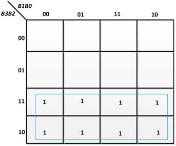
Fig. 9: K-Map for G3 in Binary to Gray Code Converter
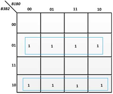
Fig. 10: K-Map for G2 in Binary to Gray Code Converter
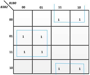
Fig. 11: K-Map for G1 in Binary to Gray Code Converter
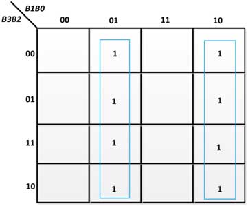
Fig. 12: K-Map for G0 in Binary to Gray Code Converter
From the above K-maps, the following boolean expressions are obtained for the output variables –
G3 = B3
G2 = B3  B2
B2
G1 = B2 B1
G0 = B1 B0
So, the digital circuit for Binary to Gray Code Converter uses EX-OR gates. It can be constructed using 7486 IC.
Gray Code to Binary Converter
For conversion of gray code to binary, the MSB is written down as it is and the subsequent bits are obtained by adding MSB (or higher place bit in binary converted number) and respective bit in the gray coded number. The circuit has four inputs (G3 G2 G1 G0) representing 4 bit gray code and four outputs (B3 B2 B1 B0) representing 4 – bit binary numbers. The converter circuit has the following truth table –
From the above truth table, the following K-Maps for the output variables are obtained –
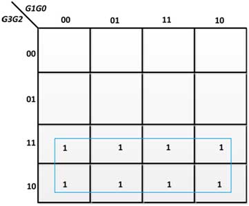
Fig. 13: K-Map for B3 in Gray to Binary Code Converter
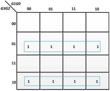
Fig. 14: K-Map for B2 in Gray to Binary Code Converter
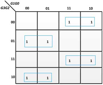
Fig. 15: K-Map for B1 in Gray to Binary Code Converter
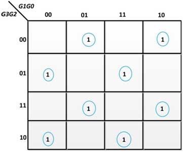
Fig. 16: K-Map for B0 in Gray to Binary Code Converter
From the above K-maps, the following boolean expressions are obtained for the output variables –
B3 = G3
B2 = G3 G2
B1 = G3 G2 G1
B0 = G3 G2 G1 G0
So, the digital circuit for Gray to Binary Code Converter uses EX-OR gates. It can be constructed using 7486 IC.
BCD to Excess-3 Converter
The 4-bit BCD numbers are same as 4-bit binary numbers. The Excess-3 coded numbers are 3 added to each BCD number. Both BCD and Excess-3 are weighted code systems. The circuit designed here converts only single digit BCD numbers to equivalent single digit Excess-3 numbers. The circuit has four inputs (B3 B2 B1 B0) representing 4 bit BCD code and four outputs (E3 E2 E1 E0) representing 4 – bit excess – 3 numbers. The converter circuit has the following truth table –
From the above truth table, the following K-Maps for the output variables are obtained –
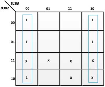
Fig. 16: K-Map for E0 in BCD to Excess-3 Code Converter
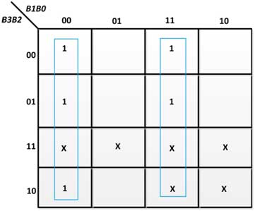
Fig. 17: K-Map for E1 in BCD to Excess-3 Code Converter
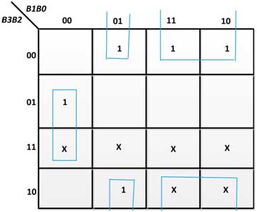
Fig. 18: K-Map for E2 in BCD to Excess-3 Code Converter

Fig. 19: K-Map for E3 in BCD to Excess-3 Code Converter
From the above K-maps, the following boolean expressions are obtained for the output variables –
E0 = B0′
E1 = B1 B0
E2 = B2 (B1 + B0)
E3 = B3 B2 (B1 B0)
So, the digital circuit for BCD to Excess-3 Code Converter uses EX-OR, AND and NOT gates. It can be constructed using 7486, 7432, 7408 and 7404 ICs.
Excess-3 to BCD Converter
The BCD coded numbers are three less than Excess-3 coded numbers. The converter circuit has four inputs (X3 X2 X1 X0) representing 4-bit excess – 3 code and four outputs (A B C D) representing 4 – bit BCD numbers. It has the following truth table –
From the above truth table, the following K-Maps for the output variables are obtained –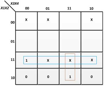
Fig. 20: K-Map for A in Excess-3 to BCD Code Converter
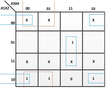
Fig. 21: K-Map for B in Excess-3 to BCD Code Converter
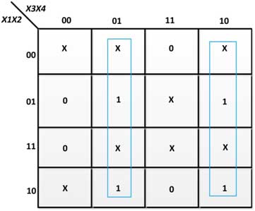
Fig. 22: K-Map for C in Excess-3 to BCD Code Converter
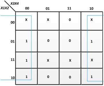
Fig. 23: K-Map for D in Excess-3 to BCD Code Converter
From the above K-maps, the following boolean expressions are obtained for the output variables –
A = X1(X2 + X3.X4)
B = X2 (X3′ + X4′)
C = X3 X4
D = X4′
So, the digital circuit for Excess-3 Code to BCD Converter uses EX-OR, AND and NOT gates. It can be constructed using 7486, 7432, 7408 and 7404 ICs.
Testing the circuits –
The circuits designed above can be tested by giving supply voltage to the ICs by a battery via 7805 voltage regulator. The same voltage can be dropped to 2V level using a variable resistor for HIGH logic while providing LOW logic through ground. The output signals can be checked by connecting LEDs at the output pins of each converter circuit. The circuits can be checked by verifying truth tables for each circuit.
In the next tutorial, learn to design bit magnitude comparator.
Project Source Code
Circuit Diagrams


Filed Under: Electronic Projects

Questions related to this article?
👉Ask and discuss on EDAboard.com and Electro-Tech-Online.com forums.
Tell Us What You Think!!
You must be logged in to post a comment.