A CCD can be thought of as a subset of Charge Transfer Devices. These are based upon Metal Oxide Semiconductor (MOS) capacitors. Two types, viz surface channel and buried channel MOS capacitors have been used in CCD, but primarily buried channel capacitors have been used for manufacturing since these do not have problems caused by surface irregularities at oxide-semiconductor interface. A thin n-type buried channel is formed on a p-type substrate through ion implantation. The Silicon Dioxide insulator layer is grown on top of the n-region, and to complete the capacitor, gates of metal or heavily doped polycrystalline silicon are placed on top of the insulating SiO2 using CVD process. To isolate the charge packets of one column from other, thermally grown oxide ‘channel stops’ are placed parallel to the channels.

Buried Channel MOS
But if a CCD cell were to pass along charges, it would just be any other MOS capacitor. The additional property that it is sensitive to light makes a CCD unique. The response to photons is through the epitaxial layers of doped silicon grown on the substrate. When photons are incident on the semiconductor surface, they dislodge electrons which create charge that is proportional to the light falling on the surface. A single CCD cell performs four functions:
1. Receive charge from the cell above it in the array.
2. Hold that charge for sometime without much loss.
3. Pass that charge to the cell below it in array.
4. Respond to outside stimulus like light and generate its own charge.
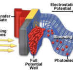
There lies the main challenge, to read out these charges. Many schemes named binning, two-phase, three-phase, four-phase etc. corresponding to the type of clocking used have been used for transferring the charge packets cell to cell in the bucket brigade style while protecting the integrity of each packet. Considering a 3-phase scheme, there would be 3 control wires passing each cell, each wire being connected to one phase of the clock. These wires control the height of the potential wells which pushes and pulls the charge packets along the line. For a three-phase scheme, each pixel contains one storage and two barrier gates. Each storage gate is connected to the same phase and sequentially, every barrier gate is connected to their respective phase clocks. A charge packet moves from one region into the next region when the second gate goes to a higher potential and the first gate goes low. This sequential movement of charges can be demonstrated as in the figure below.

Attempts were made to use CCD devices as memory devices. But soon after, other techniques took over and after that CCD devices have been used primarily in scanning, microscopy and photography. One dimensional array has been utilized in flatbed scanners where one line is scanned at a time and the charges are read out after that. The array is moved mechanically over the entire page to create the 2 dimensional scanned images. Two dimensional arrays have been used to capture the entire scene in one go and then transfer the charges to the output.
 One dimensional linear array CCD
You may also like:
Filed Under: Articles

Questions related to this article?
👉Ask and discuss on Electro-Tech-Online.com and EDAboard.com forums.
Tell Us What You Think!!
You must be logged in to post a comment.