Engineers Garage

  • Projects and Tutorials
    • Electronic Projects
      • 8051
      • Arduino
      • ARM
      • AVR
      • PIC
      • Raspberry pi
      • STM32
    • Tutorials
    • Circuit Design
    • Project Videos
    • Components
  • Articles
    • Tech Articles
    • Insight
    • Invention Stories
    • How to
    • What Is
  • News
    • Electronic Products News
    • DIY Reviews
    • Guest Post
  • Forums
    • EDABoard.com
    • Electro-Tech-Online
    • EG Forum Archive
  • Digi-Key Store
    • Cables, Wires
    • Connectors, Interconnect
    • Discrete
    • Electromechanical
    • Embedded Computers
    • Enclosures, Hardware, Office
    • Integrated Circuits (ICs)
    • Isolators
    • LED/Optoelectronics
    • Passive
    • Power, Circuit Protection
    • Programmers
    • RF, Wireless
    • Semiconductors
    • Sensors, Transducers
    • Test Products
    • Tools
  • EE Resources
    • DesignFast
    • LEAP Awards
    • Oscilloscope Product Finder
    • White Papers
    • Webinars
  • EE Learning Center
    • Design Guides
      • WiFi & the IOT Design Guide
      • Microcontrollers Design Guide
      • State of the Art Inductors Design Guide
  • Women in Engineering

CD 4013 based Sound Sensing Module

By Ashutosh Bhatt

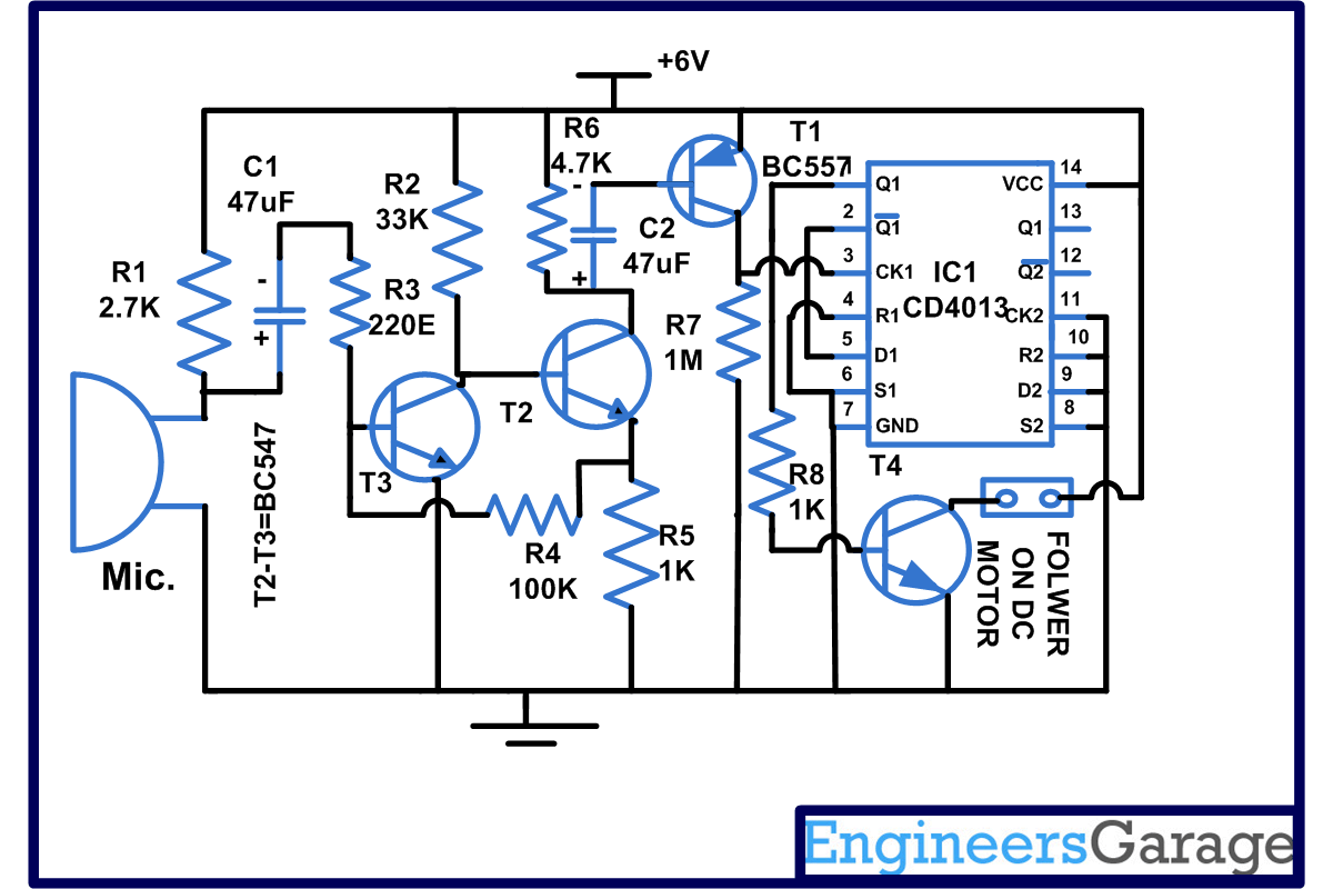
In this circuit when you clap or whistle in front of a Mic, a flower connected in the output starts rotating. For making this sound sensor circuit, we have used CD4013 IC, DC motor and few more components. IC CD4013 contains two independent D type flip flop which exist in one of two states and can store information. Each module is further equipped with a group of  pin outs assigned as data, set, reset, clock input and a couple of complementary outputs Q and . As we know, it has couple of output that change or toggle state as response to trigger applied to input terminals.  

To put in simple words, this circuit describes movement of a DC motor based on the voice sensing capabilities provided to it through a microphone. The DC motor can be accessorized using a variety of attachments such a miniature flower (in this case), a small fan etc. Accessorizing can get more diverse when power of DC motor is increased but this might make the circuit bulkier in terms of power requirements and power handling capacity of the IC might get tested too. 


CD 4013 comes in 14 pin dual inline package. To understand the working of circuit first we have to understand its pin lay out.

Fig. 1: Pin Diagram Of CD 4013 IC

1. Pin no1, 2, 13 and 12 are complimentary outputs. This set of output changes state while setting and resetting the IC producing opposite logic level at any instant when operated in bistable mode.

2. Pin 5 and 9 are called Data pins and are generally connected to one of the outputs  for the purpose of lengthening the applied input clock for square wave. For other waves, they may be terminated to any other logic level or they may be connected either connected to supply or to the ground of the circuit. In this circuit we have connected {C}{C}{C}{C}{C}{C}{C}{C}{C}{C}

 and Data pin 5 together.

3. Pin 3 and 11 are called as Clock input.  These are input pins which are used to receive clock signals generally in the form of square wave. These signals may be provided by the transistor in the form of astable multivibrator or with the help of NAND or NOR gate. This input will produce effect on any of the output pins, the other being connected to Data pin as explained above. In our circuit we are providing clock signal through transistor circuit.

4. Pin 4, 6 and 10, 8 are called as set and reset pins. Whenever any of the pin goes high, we will get the output. When set and reset are low, output shows that data at input at the time of last low to high clock transition means output is held till the next transition.  For safety, these are also assigned to a logic level generally they are grounded with a high value resistor. Once this is done, the input can be made to alternately respond to positive peak pulses to toggle the logic stage of the Q and {C}{C}{C}{C}{C}{C}{C}{C}{C}{C}

 output alternately.

5. Pin 14 and 7 are called supply and ground pin respectively. Pin 14 receives the positive supply input which should not exceed 15V otherwise it will destroy the IC and pin 7 is ground or connected to negative supply input of IC.

Now you can also see this in truth table-


CLK

D

R

S

Q

Q-

low-hi

0

0

0

0

1

Low-high

1

0

0

1

0

Hi- low

X

0

0

Q

Q

X

X

1

0

0

1

X

X

0

1

1

0

X

X

1

1

1

1

Now working of this sound sensing circuit is very simple: when you clap in front of the Mic, signals are amplified by the transistor and clock input of the IC makes its transition from low to high. We will receive a high at output Q, transistor connected to it will conduct and a DC motor connected to it will start rotating. At this time we will receive low at{C}{C}{C}{C}{C}{C}{C}{C}{C}{C}

. We have also connected pin 2 and 5 together for the purpose of lengthening the clock pulse as explained above. Pins 9, 10, 11 are also connected to ground so that will not produce any false pulse.

Circuit Diagrams

Circuit-Diagram-CD-4013-based-Sound-Sensing-Module

Project Components

  • Capacitor
  • Resistor
  • Transistor BC547


Filed Under: Electronic Projects
Tagged With: cd 4013, clap, ic, voice sensing
 

Questions related to this article?
👉Ask and discuss on EDAboard.com and Electro-Tech-Online.com forums.


Tell Us What You Think!! Cancel reply

You must be logged in to post a comment.

HAVE A QUESTION?

Have a technical question about an article or other engineering questions? Check out our engineering forums EDABoard.com and Electro-Tech-Online.com where you can get those questions asked and answered by your peers!


Featured Tutorials

  • PS2 Keyboard To Store Text In SD Card Using Arduino Circuit Setup On Breadboard
    How To Use PS2 Keyboard To Store Text In SD Card Using Arduino- (Part 42/49)
  • Wireless Path Tracking System Using Mouse, XBee And Arduino Circuit Setup On Breadboard
    How To Make A Wireless Path Tracking System Using Mouse, XBee And Arduino- (Part 43/49)
  • How to Make a Wireless Keyboard Using Xbee with Arduino- (Part 44/49)
  • Making Phone Call From GSM Module Using Arduino Circuit Setup On Breadboard
    How to Make Phonecall From GSM Module Using Arduino- (Part 45/49)
  • How to Make a Call using Keyboard, GSM Module and Arduino
    How To Make A Call Using Keyboard, GSM Module And Arduino- (Part 46/49)
  • Receiving SMS Using GSM Module With Arduino Prototype
    How to Receive SMS Using GSM Module with Arduino- (Part 47/49)

Stay Up To Date

Newsletter Signup

Sign up and receive our weekly newsletter for latest Tech articles, Electronics Projects, Tutorial series and other insightful tech content.

EE Training Center Classrooms

EE Classrooms

Recent Articles

  • Renesas delivers intelligent sensor solutions for IoT applications
  • Microchip Technology releases AVR-IoT Cellular Mini Development Board
  • Qualcomm acquires Cellwize to accelerate 5G adoption and spur infrastructure innovation
  • MediaTek’s chipset offers high-performance option for 5G smartphones
  • Nexperia’s new level translators support legacy and future mobile SIM cards

Most Popular

5G 555 timer circuit 8051 ai Arduino atmega16 automotive avr bluetooth dc motor display Electronic Part Electronic Parts Fujitsu ic infineontechnologies integratedcircuit Intel IoT ir lcd led maximintegratedproducts microchip microchiptechnology Microchip Technology microcontroller microcontrollers mosfet motor powermanagement Raspberry Pi remote renesaselectronics renesaselectronicscorporation Research samsung semiconductor sensor software STMicroelectronics switch Technology vishayintertechnology wireless

RSS EDABOARD.com Discussions

  • Thermal pad
  • lna+mixer noise figure problem
  • ADS Cascode Power Amplifier Loadpull Problem
  • SMPS topology
  • DC DC converter output voltage rise time

RSS Electro-Tech-Online.com Discussions

  • Where is the fuse ?
  • 500+V power supply from 9V battery using ZVS
  • Control Bare LCD With ATmega328p
  • undefined reference header file in proteus
  • Engine compression high voltage ignition voltage?
Engineers Garage
  • Analog IC TIps
  • Connector Tips
  • DesignFast
  • EDABoard Forums
  • EE World Online
  • Electro-Tech-Online Forums
  • Microcontroller Tips
  • Power Electronic Tips
  • Sensor Tips
  • Test and Measurement Tips
  • 5G Technology World
  • About Us
  • Contact Us
  • Advertise

Copyright © 2022 WTWH Media LLC. All Rights Reserved. The material on this site may not be reproduced, distributed, transmitted, cached or otherwise used, except with the prior written permission of WTWH Media
Privacy Policy | Advertising | About Us

Search Engineers Garage

  • Projects and Tutorials
    • Electronic Projects
      • 8051
      • Arduino
      • ARM
      • AVR
      • PIC
      • Raspberry pi
      • STM32
    • Tutorials
    • Circuit Design
    • Project Videos
    • Components
  • Articles
    • Tech Articles
    • Insight
    • Invention Stories
    • How to
    • What Is
  • News
    • Electronic Products News
    • DIY Reviews
    • Guest Post
  • Forums
    • EDABoard.com
    • Electro-Tech-Online
    • EG Forum Archive
  • Digi-Key Store
    • Cables, Wires
    • Connectors, Interconnect
    • Discrete
    • Electromechanical
    • Embedded Computers
    • Enclosures, Hardware, Office
    • Integrated Circuits (ICs)
    • Isolators
    • LED/Optoelectronics
    • Passive
    • Power, Circuit Protection
    • Programmers
    • RF, Wireless
    • Semiconductors
    • Sensors, Transducers
    • Test Products
    • Tools
  • EE Resources
    • DesignFast
    • LEAP Awards
    • Oscilloscope Product Finder
    • White Papers
    • Webinars
  • EE Learning Center
    • Design Guides
      • WiFi & the IOT Design Guide
      • Microcontrollers Design Guide
      • State of the Art Inductors Design Guide
  • Women in Engineering