The frequency modulation (FM) is one of the widely used modulation technique in wireless transmission. They are most commonly used in high quality radio transmission from FM radio stations. The main advantage of the frequency modulation technique is the very high signal to noise ratio that can be achieved on the received signals.
In the technique of frequency modulation the frequency of a carrier wave is modulated according to the variations in the amplitude of the message wave. Unlike the amplitude modulation technique the amplitude of the carrier signal remains same. The receiver tracks for the change in the frequency of the received signal only and the amplitude variations due to the noise does not make any changes in the receiver output. Hence quality of the signal produced at the output of the receiver is very high compared to other modulation techniques.
This article demonstrates the generation of frequency modulated waveform in the simplest possible way. Here a Wien Bridge oscillator based circuit is used to generate pure sine wave which is then used to modulate the frequency of the waves produced by a 555 timer IC.
DESCRIPTION:
The 555 is an 8 pin versatile timer IC which can be wired to make thousands of verity circuits. The 555 can be used as monostable, bistable or astable multivibrator circuits. They are most commonly used as an astable multivibrator which can continuously produce pulses at constant intervals of time. The 555 IC requires only few components which can be connected to their pins and the output pulse waveform can be obtained from the pin3 of the 555 IC.
The pinout of the 555 IC is shown in the following figure:

Fig. 1: Pin-Out Diagram Of 555 IC
The pin number 1 and 8 are used to supply the ground and VCC to the IC respectively. The pin number 2, 6 and 7 are used according to the timing requirements of various pulse generating circuits. The pin number 4 can be used to reset IC. The pin number 3 provides the output pulse from the 555 timer IC. The pin number 5 the pin which can change or modulate the pulse frequency produced at the pin number 3.
In this project the 555 is wired as an astable multivibrator to produce continuous square waves with a fixed time period. The sine wave generated using the Wien Bridge oscillator applied to the pin number 5 of the 555 timer IC to modulate the frequency of the generated pulses. Since the output of a Wien Bridge oscillator is a pure sine wave having both the positive and negative half cycles they should not be directly applied to the 555 which works on positive DC voltage only. The entire sinusoidal waveform should be clamped to the positive voltage side before it is applied to the 555 modulator circuit so as to get the output response for both the half cycles. Hence the entire circuit can be divided into three separate blocks:
1) Sine wave generator using Wien Bridge oscillator
2) Positive clamper
3) Frequency modulator using 555
The block diagram of the entire circuit is shown in the following diagram:

Fig. 2: Block Diagram Of Frequency Modulated Waveform Generation
{C 1) Variable frequency sine wave generator
A sine wave generator circuit is used in this project which is based on the Wien Bridge oscillator circuit. The Wien Bridge oscillator circuit can produce distortion less sinusoidal sweep at its output. The circuit is designed in such a way that both the amplitude and frequency of the oscillator can be adjusted using potentiometers.
The circuit diagram of the variable frequency sine wave oscillator is shown in the following:

Fig. 3: Circuit Diagram Of Variable Frequency Sine Wave Oscillator

Fig. 4: Variable Frequency Sine Wave Oscillator Circuit On Breadboard
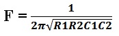
The frequency of the above circuit can be varied by simply varying the potentiometer R2 and the amplitude of the wave form can be adjusted by varying the potentiometer R. The frequency of the sine wave generated by the above circuit depends on the components R1, R2, C1 and C2 and the equation for the frequency is given below:
For the ease of adjusting the amplitude of the wave to obtain proper sinusoidal sweep, a coarse and fine adjustment has been implemented using potentiometers. A low value (1K) potentiometer is connected in series with the high value (100K) potentiometer so that the coarse adjustment can be done with the high value resistor and the fine adjustment with the low value resistor.
Positive Clamper
2) POSITIVE CLAMPER
A clamper circuit must be used to shift the entire sinusoidal waveform to the positive voltage side so that the 555 modulator circuit can produce corresponding output response. The clamping circuit requires only a diode and a capacitor and in the case of positive clamping the positive end of the diode is grounded and the wave is received at the other end through a capacitor. The circuit of the positive clamper is shown below:

Fig. 5: Circuit Diagram Of Positive Clamper
The above circuit forms the simplest positive waveform clamper, but it cannot be directly used in most of the circuits since it cannot be loaded. When a load of very small resistance is applied at the output end of the circuit it may not work properly. Hence a buffer (current amplifier) must be added at the output end of the circuit as shown in the following diagram:
Fig. 6: Circuit Diagram Of Positive Clamper With Buffer(Current Amplifier) At Output
The image of the circuit wired in the breadboard is given in the following:
 At Output")
Fig. 7: Positive Clamper With Buffer(Current Amplifier) Circuit On Breadboard
The input of the clamper circuit with the current amplifier is provided with a pure sine wave input from the previous sine wave generator circuit. The following circuit diagram shows the combined circuit made by connecting the sine wave generator and the positive clamping circuit together.

Fig. 8: Circuit Diagram Of Sine Wave Generator connected with Positive Clamper Circuit
The variable frequency sine wave generator adjusted in such a way that it will generate a pure sine wave of 1 KHz. The input and output waveforms of the above circuit observed in CRO are given in the following figures:
The input waveform:

Fig. 9: Positive Clamped Input Waveform On CRO
The positive clamped output waveform:

Fig. 10: Positive Clamped Output Waveform on CRO
It can be noticed from the above image is that a small portion of the clamped waveform is still beneath the 0 voltage. The amplitude of the waveform below the 0 voltage will be exactly equal to the bias voltage of the diode used and in this case since the 1N4148 is used the amplitude of waveform in the negative side will be 0.3V.
555 Modulator Circuit
3) 555 FREQUENCY MODULATOR
The 555 is wired as a normal astable mutivibrator with constant on-off time period. The only difference in this modulator circuit is that the pin number 5 is not connected to the positive via a capacitor, but it is used to receive the modulating signal. The circuit diagram of the 555 modulator is given in the following diagram:

Fig. 11: Circuit Diagram Of 555 modulator
The pin number 4, which is the reset pin, is connected to the VCC. The pin 2 which is the trigger pin and the pin 6 which is the threshold pin is shorted together and a capacitor is connected across this point and the ground. This capacitor charges towards VCC through the diode ‘D’ and the resistor ‘R1’ and discharges from the pin 7 through the resistor ‘R2’. The charging time depends on the value of the capacitor and the value of the resistor ‘R1’ and the discharging time depends on the value of the capacitor and the value of the resistor ‘R2’. The on-off time period of the output pulse depends on the charging and the discharging time of the capacitor. Since in this circuit the R1 and R2 has the same value the charging and discharging time is same and also the on-off time period of the output pulse are same.
The 555 modulator circuit is connected with the previous positive clamper circuit through a 1uF polarized capacitor. The entire circuit diagram and the image of the circuit wired in the bread board is shown in the following figures:

Fig. 12: Circuit Diagram Of Frequency Modulated Waveform Generation

Fig. 13: Frequency Modulated Waveform Generation Circuit On Breadboard
As the amplitude variations occurs in the sine wave the frequency generated by the 555 changes and hence a frequency modulated wave is obtained at the output of the 555 IC. As the amplitude increase the frequency decreases and vice versa. For large amplitude signals the frequency variation will be large and for small amplitude signals the frequency variations will be small. The amplitude of the sine wave signal applied to the 555 modulator can be varied by varying the 1M ohm potentiometer.The following is the image captured from the dual channel CRO where the FM wave is displayed in above and the original sine wave which is used to modulate them is displayed below.

Fig. 14: Waveform of FM Wave And Original Sine Wave On CRO Screen
Filed Under: Circuit Design

Questions related to this article?
👉Ask and discuss on Electro-Tech-Online.com and EDAboard.com forums.
Tell Us What You Think!!
You must be logged in to post a comment.