The AM modulation is a kind of modulation technique which is in use since the very early days of wireless data transmission. In a radio transmission system there is a relation between the ranges of frequencies which can be transmitted wirelessly with the length of the transmitting antenna. The relation is inversely proportional to one another, means as the frequency of the signal to be transmitted increases the length of the antenna can be reduced and as the frequency of the signal to be transmitted decreases the length of the transmitting antenna should be increased accordingly.
Using an antenna of few meters the frequencies in the range of Mhz can be easily transmitted to a distance. The basic purpose of the wireless transmitting system in early days was to transmit the audio signals, but to transmit audio signals which fall in the range of few Khz an antenna of more than a kilometer height would have been required. Since it was practically impossible to construct such a long antenna, the high frequency signals are transmitted after they are modulated with the low frequency audio signals.
The amplitude modulation is the simplest modulation technique among the wide verity of modulation techniques in use. The amplitude modulation of a high frequency signal is easy to achieve and the demodulation is also simple compared to other techniques. The high frequency signal which is modulated to carry the low frequency audio signals are called ‘carrier frequency’ and the audio signals used for modulation is called ‘modulating signal’ or ‘message signal’ or ‘base band signal’. This article demonstrates how to generate an Amplitude Modulation (AM) using the simplest possible circuit.
DESCRIPTION:
To demonstrate the AM modulation of a carrier signal with a message signal, both the carrier signal and message signal generating circuits are also made and the details of them will be discussed in the subsequent section. The carrier signal and message signal used in this project are pure sine waves. Hence the entire circuit can be divided into three blocks:
1. Carrier frequency generator (High frequency sine wave)
2. Message frequency generator (Low frequency sine wave)
3. AM Modulator.
The block diagram of the AM modulation used in this project is shown in the following diagram;
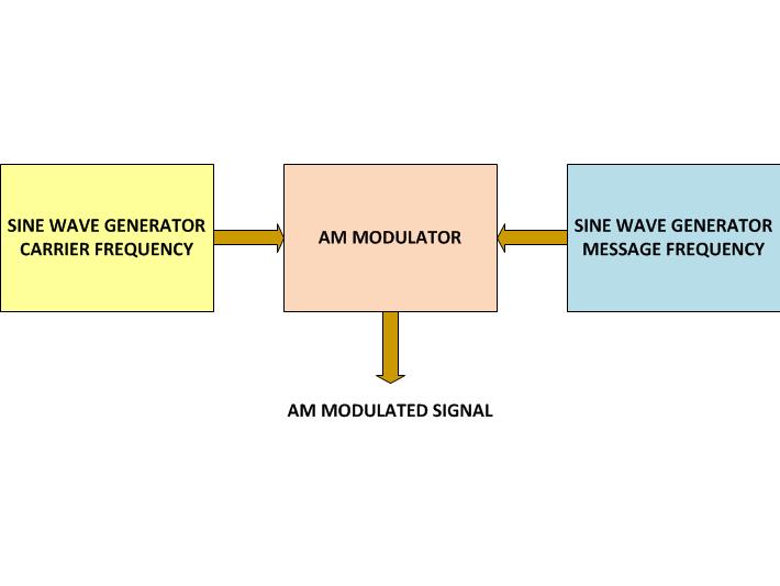
Fig. 1: Block Diagram Of AM Modulation
For both the carrier signal of high frequency and the message signal of low frequency, exactly same sine wave generating circuits are designed but the frequencies are set to high and low respectively with the help of their variable components. Hence this project has two similar variable frequency sine wave generator circuits and an AM modulator circuit.
Variable frequency sine wave generator
The sine wave generation circuit used in this project is the Wien bridge oscillator circuit. This is the only circuit which can generate the pure sine wave without any distortion. The amplifier component used in the Wien bridge circuit is an op-amp with dual-power supply. Both the circuits are built around the versatile op-amp IC, 741. The circuit of the sine wave generator is shown in the following figure.
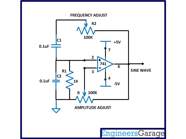
Fig. 2: Circuit Diagram Of Sine Wave Generator
The frequency of the above circuit can be varied by simply varying the potentiometer R2 and the amplitude of the wave form can be adjusted by varying the potentiometer R. The frequency of the sine wave generated by the above circuit depends on the components R1, R2, C1 and C2 and the equation for the frequency is given below;

The image of the circuit made for generating the carries signal is shown below;
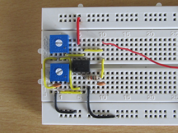
Fig. 3: Carries Frequency Generator (High-Frequency Waves) Circuit On Breadboard
The circuit is then adjusted to generate a high frequency sine wave and which can be observed in a CRO as shown in the following image;
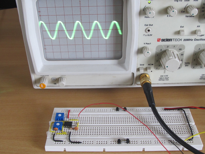
Fig. 4: Carrier Frequency Waveform in AM Modulation Displayed On CRO
An exactly similar circuit is wired again in the bread board and this time the circuit is adjusted to generate a low frequency sine wave. The two sine wave generating circuits wired in a bread board is shown in the following image;
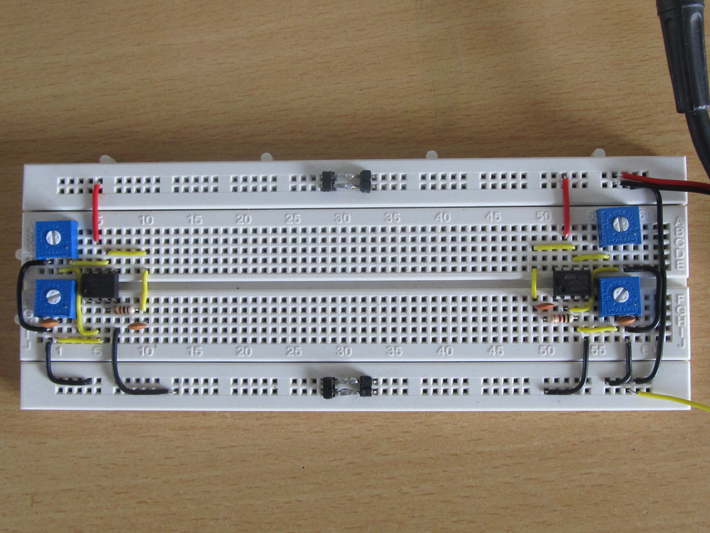
Fig. 5: Two Sine Wave Generating Circuit On Breadboard
Variable Sine Wave Generator
The wave generated by the two circuits can be connected to the CRO using the two channels of CRO and can be observed together in the CRO screen. In the following figure the high frequency and low frequency sine waves displayed in the CRO screen is shown;
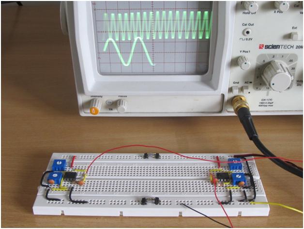
Fig. 6: High Frequency And Low Frequency Sine Waves Displayed On CRO Screen
The Wien bridge circuits shown in the above picture can be tuned for a range of frequency which can be calculated using the frequency equation mentioned above. According to the frequency equation the frequency depends on the values of R1, R2, C1 and C2 and since the resistance R1 and the capacitance C1 and C2 have fixed values in the circuit, the frequency can be adjusted by varying the resistance of the potentiometer R2 alone. The potentiometer R2 is selected as 100K so as to generate wide frequency range. As the value of R2 increases the frequency decreases according to the frequency equation. The circuit is designed to produce frequencies above 100 Hz only and hence the values of the other components which affect the frequency are selected accordingly. When the value of R2 is at its maximum i.e 100000 ohms, the design requires frequency above 100 Hz;

From the above equation R1*C1*C2 < 2.5*10^-11. The value of the resistance R1 is selected randomly as 1K and decided to use the same value for C1 and C2 which can be calculated from the previous relation as < .15*10^-6. Hence the values of capacitors are selected as 0.1uF.
The R2 can be varied to a maximum of 100K ohms and using the frequency equation the corresponding frequency can be calculated as follows;
R1 = 1000 ohms
R2 = 100000 ohms
C1 = 0.1*10^-6
C2 = 0.1*10^-6

The experimentally observed minimum frequency using this circuit is 166 Hzwhich is very close to the theoretical value.
According to the frequency equation when the R2 is zero the circuit will generate infinite frequency, but practically that is not possible. The minimum value of the R2 which can generate a distortion less sine wave is tested and found to be 130 ohms. At this low value of the R2 the circuit will produce the maximum frequency and it can be calculated using the frequency equationas shown below;

The experimentally observed maximum frequency using this circuit is at the same value of R2 is 4166 Hz which justifies the calculation. Hence using the Wien bridge variable frequency sine wave generator circuit, one can easily generate a sine wave with a frequency in the range of 200 Hz to 4 KHz.
For the purpose of the demonstration of AM modulation one circuit is tuned to generate a high frequency around 4 KHz and the other circuit is tuned to generate a frequency of around 500 Hz. The 4 KHz circuit acts as the carrier generator and the low frequency 500 Hz sine wave circuit acts as the message signal generator.
AM Modulator
AM modulator
There are different kinds of circuits which can produce AM modulation. The most common among them are transistor based circuits. The transistor based circuits requires proper biasing and a single transistor in most of the cases is not enough to handle both the positive and negative cycles of large amplitude signals. There are inductors or coil based circuits which can also produce AM modulation but they also require proper tuning and they are vulnerable to noise in the surroundings.
The simplest and the stable AM modulator circuit can be designed with the help of an FET. The carrier wave can be allowed to flow through the channel of the FET and the message signal can be used to modify the width of the channel and hence one can achieve the simplest AM modulation.
The component used here as an AM modulator is the N-channel FET, BFW10. The carrier signal is fed through the N-channel from source to drain of the FET which is then modulated by applying the message signal on the gate of the FET. The circuit built around BFW10 which can act as an AM modulator is shown in the following image;
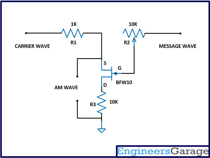
Fig. 7: Circuit Diagram Of AM Modulator Built From N-channel FET, BFW10
Compared to other circuits there is no complex calculations involved in the design of the components used in this circuits. R1 is used as the current limiting resistor and the resistor R3 is used to generate a reasonable voltage drop when the AM signal current flow through it so that one can get the AM signal voltage across it. R3 is again the current limiting resistor for the base of the FET and it is selected as a potentiometer so that by varying it the depth of the modulation can be demonstratedas varying.The depth of the modulation simply means the amount of message signal amplitude that is required to be present in given amplitude of the carrier signal.The carrier wave is applied through the resistor R1 to the FET and the message wave is applied to the gate of the FET through the potentiometer R2. The potentiometer R2 can be varied to adjust the depth of the modulation. The circuit built for the AM modulator using BFW10 is shown in the following image;
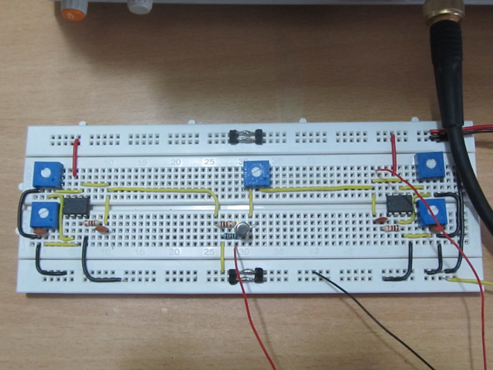
Fig. 8: AM Modulator using BFW10 Circuit On Breadboard
The carrier signal flows through the N-channel of the FET and as they flows the message signal voltage at the gate of the FET continuously increases and decreases the width of the N-channel. Thus the carrier signal flowing through the channel experiences an increase and decrease in resistance corresponding to the increase or decrease of the amplitude of the message signal. Henceforth the amplitude of the carrier signal varies according to the message signal as it flows through the N-channel. This modulated amplitude carrier signal appears across the source of the FET and ground as AM wave.
The AM wave generated by the circuit and displayed in the in CRO is shown in the following images;
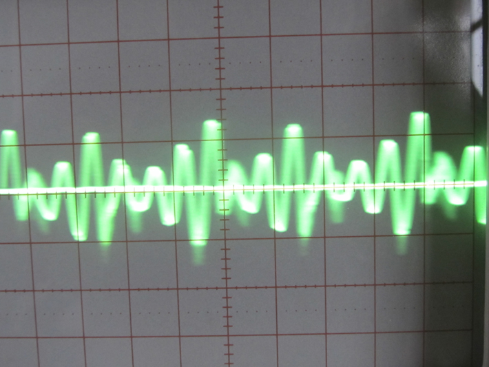
Fig. 9: AM Wave Generated by AM Modulator Circuit Displayed on CRO
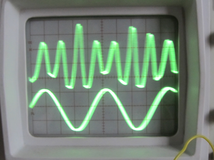
Fig. 10: AM Wave Generated by AM Modulator Circuit Displayed on CRO Screen
The complete circuit for the AM generation
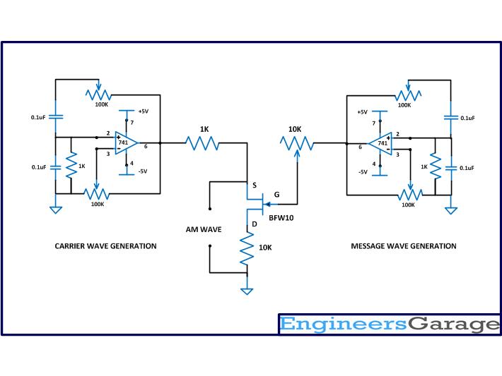
Fig. 11: Circuit Diagram of AM Generation
Filed Under: Circuit Design


Questions related to this article?
👉Ask and discuss on Electro-Tech-Online.com and EDAboard.com forums.
Tell Us What You Think!!
You must be logged in to post a comment.