The simple pulse modulation technique called Pulse Amplitude Modulation (PAM) proved to be more power efficient than the PWM and consumes constant power for individual pulses like PPM. In PAM the amplitude of the individual pulses are varied according to the amplitude of the modulating signals. The PAM modulator and demodulator circuits simple compared to other kind of modulation and demodulation techniques. There are two kinds of PAM one in which the pulses have the same polarity and the other in which the pulses can have both positive and negative polarity according to the amplitude of the modulating signal.
The PAM modulation technique is widely used in high speed digital communications like telephone modems, Ethernet etc. They are used to drive LED lights more efficiently than using PWM method. Unlike the PPM the transmitter and receiver synchronization is not required for the PAM. This article discusses about the demodulation of Pulse Amplitude Modulated signals with the help of simplest possible circuit.
DESCRIPTION:
The demodulator circuit explained in this article can extract the modulating signal from the Single Polarity PAM wave. The message signal used here is a pure sine wave generated using Wien Bridge Oscillator (WBO) and an FET based modulator circuit is used for the PAM modulation. The demodulation of the PAM signals can be done easily using a Low-pass filter.
")
Fig. 1: Block Diagram Of Pulse Amplitude Modulation (PAM)
{ 1) Variable frequency sine wave generator
A sine wave generator circuit is used in this project which is based on the Wien Bridge Oscillator (WBO) circuit. The Wien Bridge oscillator circuit can produce distortion less sinusoidal sweep at its output. The circuit is designed in such a way that both the amplitude and frequency of the oscillator can be adjusted using potentiometers.
The circuit diagram of the variable frequency sine wave oscillator is shown in the following:
Fig. 2: Circuit Diagram Of Variable Frequency Sine Wave Oscillator
The frequency of the sine wave generated by the above circuit depends on the components R1, R2, C1 and C2 and the equation for the frequency is given below:
Fig. 3: Variable Frequency Sine Wave Oscillator Waveform Generation on CRO Screen
2) SQUARE WAVE GENERATOR
The square wave is generated in this project using an op-amp based astable circuit. The op-amp based astable circuit is used to generate the square wave due to the less number of components required and less complex circuit. The ON-time and the OFF-time of the pulses can be made identical and the frequency can be easily adjusted without changing them. However in this project the circuit is designed to be producing a constant frequency. The astable multivibrator circuit using op-amp 741 is given below.
Fig. 4: Circuit Diagram Of Stable Multivibrator with Op-Amp 741
The time period of the pulses generated by the above circuit depends upon the values of the resistor R and the capacitor C. The following equation gives the approximate time period of the pulses generated by the op-amp astable multivibrator circuit.
T = 2.2 * R*C
PAM Modulator and LPF
3) PAM MODULATOR
The PAM modulator circuit in this project has to modify the amplitude of the pulses having a frequency of 45 KHz with the modulating sine wave of frequency 1 KHz. The modulator here is realized using a simple FET and a couple of resistors. The FET used here is BFW10 which is an N-channel FET and since it is a unipolar device it is suitable for applications in which the signals having both positive and negative polarities are used.
Fig. 5: Circuit Diagram Of PAM Modulator
Fig. 6: PAM Modulator Waveform on CRO Screen
4) LOW PASS FILTER
The Low-pass filter for the PAM modulator is designed in such a way that the time constant of the filter matches with the time period of the modulating signal. Since 1KHz sine wave is used as modulating signal, the time constant of the low pass filter using the RC circuit is 1 ms. Assuming the value of the resistor ‘R’ as 1K, then the capacitor selected should be of 1uF so that the time constant will be exactly 1 ms.
The circuit diagram of the Low pass filter made up of a single resistor and a capacitor is given in the following figure:

Fig. 7: Circuit Diagram Of Low-Pass Filter

Fig. 8: Low-Pass Filter Circuit On Breadboard
The Low pass filter simply avoidsthe entire high frequency component to appear at its output but allows the low frequency component of the message signal to pass through it. Thus the Low pass filter can separate out the message signal from the high frequency pulses whose amplitude are modulated according to the amplitude of the message signal.
As the order of the filter increases the quality of the message signal recreated will also increase. Usually the low pass filter in the PAM demodulator circuit follows by an amplifier circuit. The PAM demodulator circuit with the first order low pass filter used for the demodulation is given in the following figure.
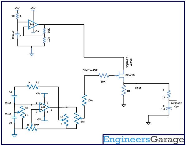
Fig. 9: Circuit Diagram Of PAM Demodulator Using Low-Pass Filter

Fig. 10: PAM Demodulator with Low-Pass Filter Circuit On Breadboard
The dual channel CRO displaying both the actual modulating sine wave for the PAM and the demodulated wave from output from the PAM demodulator circuit is shown in the following image:
Fig. 11: Waveform Of Actual modulating Sine Wave For PAM And Demodulated Output From PAM Demodulator Circuit
Filed Under: Circuit Design, More Editor's Picks

Questions related to this article?
👉Ask and discuss on Electro-Tech-Online.com and EDAboard.com forums.
Tell Us What You Think!!
You must be logged in to post a comment.