Step: 3 Functional blocks into block diagram
Up to this point we were developing the basic functions into specific functional blocks according to their requirements. Let’s take a look at what all functional blocks we have, it will give you an idea how far we advanced in the designing process.

Fig. 1: Block Diagram of Basic Functional Blocks For Designing Process
Let’s take a quick look at the details of the blocks shown in the above figure.
|
BLOCK |
NAME |
FUNCTION |
|
A |
RELAYS |
Switching the audio video signals using relays |
|
B1 |
IR PHOTODIODE |
Produce output according to IR light intensity |
|
B2 |
COMPARATOR |
Level detection of IR light from the TV remote |
|
C1 |
MONOSTABLE SMALL |
Continuous output from pulse train input |
|
C2 |
MONOSTABLE LARGE |
Trigger an output after a period of continuous input |
|
D1 |
BISTABLE |
Toggles the output for each and every input |
|
D2 |
DRIVER |
Current amplification for driving the relays |
Table: basic blocks and functions
Each of the blocks shown above can perform their own specified functions only. The entire blocks should perform together to give us a collective output. It will happen only when we connect the blocks together in the proper way. Next we are going to discuss how to connect these blocks together so that we have a complete block diagram for the device.
From the entire discussion so far you might already have a picture about the way of connecting these blocks together. The IR light from the TV remote triggers the working of the device and who receives the IR light pulses from the TV remote, the IR photodiode. Hence the working starts at the Block B1) IR PHOTODIODE. Let’s consider it as the 1st block.
The IR PHOTODIODE blocks output is level checked by the COMPARATOR block for the rest of the circuit, hence the Block B2) COMPARATOR block should immediate block after the Block B1). Thus the Block B2) COMPARATOR becomes the 2nd block.
The COMPARATOR block’s output is a train of pulses which should be converted to a continuous pulse using the MONOSTABLE SMALL block. Thus we can assume that the Block C1) MONOSTABLE SMALL block should immediately follow the Block B2) and Block C1) is the 3rd block.
The MONOSTABLE SMALL block’s output is meant to be used by the MONOSTABLE LARGE block for triggering its output after its timing period. Hence the Block C2) MONOSTABLE LARGE block should be the very next block to the Block C1) and Block C2) is the 4th block.
Each and every time the MONOSTABLE LARGE block produces an output, the BISTABLE block is the one which toggles its output, hence the Block D1) BISTABLE block should immediately follow the Block C2) and Block D1) is the 5th block.
The BISTABLE block should operate the relay block and is possible only through the DRIVER block. Hence the Block D2) DRIVER block follows the BISTABLE block and it is the 6th block.
There is only one more block left which follows the DRIVER block. It is the Block A) RELAYS which becomes the 7th block.
The above brief discussion about the connecting order of the blocks is simply represented in the following table
|
ORDER |
BLOCK |
NAME |
|
1 |
B1 |
IR PHOTODIODE |
|
2 |
B2 |
COMPARATOR |
|
3 |
C1 |
MONOSTABLE SMALL |
|
4 |
C2 |
MONOSTABLE LARGE |
|
5 |
D1 |
BISTABLE |
|
6 |
D2 |
DRIVER |
|
7 |
A |
RELAYS |
Table: order of the functional blocks
Order & Explanation of Functional Blocks
Let’s connect the blocks together in the order as per the above table and such a block diagram is shown in the following figure.

Fig. 2: Block Diagram Of Connected Functional Blocks
We’ve just reached an important stage of the design process where we have the basic block diagram regarding the design of the circuit. With this simple diagram anyone can make out the way in which we are going to develop our device. Each block represents a stage and the arrow points to the very next stage in the design process.
The previous block diagram is a good reflection of our logic and plan regarding the project, but do we still missing something? Where is the power supply? Each of the blocks will eventually be developed into a complete circuit and they will require power supply. Without powers supply block the block diagram is incomplete, moreover one must know how to apply different current and voltage to different blocks.
It is important that we must apply a low voltage and regulated power supply to all the key functional blocks. The regulated power supply is important since there is lot of time critical blocks in our design. These blocks will eventually become electronic circuit and most of the electronic circuits have a tendency to vary its timing period with the variations in the supply voltage. Hence if we need constant timings and consistent operation of the circuit we must apply a regulated power supply. We can use a power supply regulator with the external power supply for this purpose.
A power supply regulator is a device which works on DC voltages and it can maintain its output precisely at a fixed voltage always even if there is significant variation in the input DC voltage. The concept is represented by the following diagram.
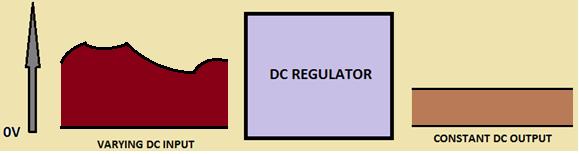
Fig. 3: Representation Of DC Regulator With Varying Input And Constant OutPut
It should be kept in mind that the DC regulator is a device which works with a power supply and hence it is not a power supply itself. It simply produces a regulated voltage at its output. This regulated voltage has low voltage and low current when compared to the power supply input. Hence normally it cannot be used with high current devices.
With all these knowledge about the DC regulator and DC power supply we can include these two blocks also in our block diagram for the design. Let us represent the regulator block as DC REGULATOR and the power supply block as EXTERNAL DC POWER. The two blocks can be represented as follows.

Fig. 4: Block of DC Power And DC Regulator
Now the question is how we are going to include the above two blocks in our previous connected blocks. We should have a good idea about which all blocks should be connected with the EXTERNAL DC POWER block and the DC regulator block.
All the blocks in our connected block diagram can be connected with the DC REGULATOR block except the DRIVER block and the RELAYS block. The DRIVER block and the RELAYS block requires more current than the DC REGULATOR block can source, hence can be connected only with the EXTERNAL DC POWER block. One more block should be connected with the EXTERNAL DC POWER block which is nothing but the DC REGULATOR block itself.
The blocks to be connected with the EXTERNAL DC POWER block and the DC REGULATOR block is mentioned in the following table
|
EXTERNAL DC POWER |
DRIVER (D2), RELAYS (A1) |
|
DC REGULATOR |
IR PHOTODIODE (B1), COMPARATOR (B2), MONOSTABLE SMALL (C1), MONOSTABLE LARGE (C2), BISTABLE (D1) |
Table: power supply and regulator connection
The connections mentioned in the above table can be included in our connected block diagram and then we can have a more solid idea about the design of the circuit. The modified block diagram with the power supply and regulator blocks included is shown below.
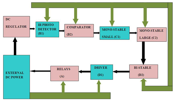
Fig. 5: Block Diagram Of Connected Blocks With Power Supply
With the above figure we have a complete picture of how to implement our design idea in this particular project. We have all the functional blocks and we have connected them together, but is that what all we need for the project? When it comes to the testing of the circuit are we going to test the entire design always with the DVD player and the set top box connected? If it seems to be not working how can we identify whether the problem is in our design or due to the TV remote simply not sending any IR light pulses?
To remove the above mentioned issues and confusions we must include suitable indicators in our design. Primarily we must assure that the device is sensing the IR light pulses from the TV remote. Hence it would be better if we include an indicator at the output section of the Block B2) COMPARATOR block so that whenever the COMPARATOR block produces output we will have an indication of it.
It won’t be comfortable always to test the output of the circuit occurs at the Block A) RELAY block with the DVD player and set top box connected to it. Then how can we test whether we are getting the correct operating signals for the RELAY block. It can be done by simply adding a suitable indicator at the input of the RELAY block, so that we can identify the driving signal input to the RELAY block.
Thus we need to modify the design by including two indicators one for the indication of IR sensing and the other for the indication of signal to the RELAY. We can consider them as separate blocks for the indicating function and let us name them as IR INDICATOR and RELAY INDICATOR respectively. The indicator blocks are shown in the following diagram.

Fig. 6: Block IR indicator And Relay Indicator
Let’s include these blocks in our modified design and with that we finish our block diagram of the design. The finished block diagram for the design of the project is shown in the following figure.

Fig. 7: Block Diagram Of All Connected Block with IR indicator And Relay Indicator
The details of the blocks shown in the final block diagram is given in the following table:
|
BLOCK |
NAME |
FUNCTION |
|
A |
RELAYS |
Switching the audio video signals using relays |
|
B1 |
IR PHOTODIODE |
Produce output according to IR light intensity |
|
B2 |
COMPARATOR |
Level detection of IR light from the TV remote |
|
C1 |
MONOSTABLE SMALL |
Continuous output from pulse train input |
|
C2 |
MONOSTABLE LARGE |
Trigger an output after a period of continuous input |
|
D1 |
BISTABLE |
Toggles the output for each and every input |
|
D2 |
DRIVER |
Current amplification for driving the relays |
|
E1 |
RELAY INDICATOR |
Indicates the status of the relay based on the signal input to the relay block from the relay driver block |
|
E2 |
IR INDICATOR |
Indicates the sensing of the IR light from the remote |
|
F1 |
DC REGULATOR |
Converts unregulated DC voltage from the external power supply to regulated DC voltage |
|
F2 |
EXTERNAL DC POWER |
Any kind of unregulated DC power supply which can be used with our design |
Table: details of blocks in the final block diagram
Finally it seems we are getting somewhere. We have finished the block diagram which represents our complete idea of developing the project. We have developed each functional block individually and finally integrated them into one single block diagram. I think the timing diagrams which we have discussed in along with the individual blocks are still in your mind. Why don’t we integrate these individual timing diagrams into a single timing diagram as we have done in the case of the block diagram? Let us do that also so that we have a complete picture about the working of the device. We will do that in the next step.
Waveforms into Timing Diagram
Step: 4 Waveforms into timing diagram
The full timing diagram which represents the working of our device is shown below. The functional bocks are shown in the left hand side and the waveforms generated with respect to time at their output are shown

Fig. 8: Waveform Timing Diagram
Let me give you one final explanation about the complete timing diagram. The functional blocks are shown on the left hand side and their output with respect to increase in time has been plotted. IR PHOTODIODE block produces an output corresponding to the light falls on it and each time the IR light from the TV remote falls on it, the IR PHOTODIODE block produces a high output. The following block is the COMPARATOR block which will compare the IR PHOTODIODE output with a predefined fixed voltage level and whenever the IR PHOTODODE output exceeds that level the output of the COMPARATOR block goes high, it happens whenever the light falls on the TV remote. Due to the pulsed nature of the IR light from the TV remote the output of the comparator will be pulsed in nature. The MONOSTABLE SMALL block which is active high will help to extend each of the pulse’s time periods so that we can have continuous pulse at the output of the MONOSTABLE SMALL block. Due to this continuous voltage at the output of the MONOSTABLE SMALL block the following block which is the MONOSTABLE LARGE which is active low can have enough time to trigger itself to its stable state. It happens only if the MONOSTABLE SMALL output is available more than a particular period of time. Each time the MONOSTABLE LARGE produces a high output the following BISTABLE block toggles its output state. The DRIVER block may have the same kind of waveform like the BISTABLE block but it can source more current to drive the RELAY block.
The explanation of the significant points in the complete timing diagram is given in the following table:
|
1 |
At the start of observation there is no IR light from the TV remote. The IR PHOTODIODE has a small voltage in its output since there is always IR light during normal room conditions. There is no output at the COMPARATOR since the IR PHOTODIODE output is still below the expected range. The MONOSTABLE SMALL is in its default stable state which is low and hence the MONOSTABLE LARGE output is also low. The BISTABLE is in its default high stable state and hence the DRIVER output is also high. |
|
2 |
TV remote transmits the pulse A and hence the output of the IR PHOTODIODE suddenly increases. This increase is above the minimum level required to trigger an output on the COMAPARATOR block and hence the COMAPARATOR also produces an output high. The pulse is maintained by the TV remote till 3 and so does the COMPARATOR output. The MONOSTABLE SMALL is triggered by the high output of the COMPARATOR block and is maintained high between 2 and 3 due to the high input. The MONOSTABLE LARGE is still in its low output state but starts the timing right from this point. The BISTABLE is in its high stable state and the DRIVER output Is also high. |
|
3 |
The pulse A from the TV remote ends at this point and the IR PHOTODIODE output falls to the normal level. Since the IR PHOTODIODE output falls below the minimum level required to trigger an output on the COMPARATOR the COMPARATOR output falls and remains low till the pulse B is generated. The MONOSTABLE SMALL output is maintained high due to its quasi stable sate between 3 and 4. The MONOSTABLE LARGE is still in its low output state but it is in its quasi stable time period. The BISTABLE is in its high stable state and the DRIVER output is also high. |
|
4 |
TV remote transmits the pulse B and hence the output of the IR PHOTODIODE suddenly increases. This increase is above the minimum level required to trigger an output on the COMAPARATOR block and hence the COMAPARATOR also produces an output high. The pulse is maintained by the TV remote till 5 and so does the COMPARATOR output. The MONOSTABLE SMALL is re-triggered by the high output of the COMPARATOR block between 4 and 5 before finishing its quasi-stable time period. Hence the MONOSTABLE SMALL output remains high. The MONOSTABLE LARGE is still in its quasi-stable low output state. The BISTABLE is in its high stable state and the DRIVER output is also high. |
|
5 |
The pulse B from the TV remote ends at this point and the IR PHOTODIODE output falls to the normal level. Since the IR PHOTODIODE output falls below the minimum level required to trigger an output on the COMPARATOR the COMPARATOR output falls and remains low till the pulse C is generated. The MONOSTABLE SMALL output is maintained high due to its quasi stable sate between 5 and 6. The MONOSTABLE LARGE is still in its low output state but it is in its quasi stable time period. The BISTABLE is in its high stable state and the DRIVER output is also high. |
|
6 |
TV remote transmits the pulse C and hence the output of the IR PHOTODIODE suddenly increases. This increase is above the minimum level required to trigger an output on the COMAPARATOR block and hence the COMAPARATOR also produces an output high. The pulse is maintained by the TV remote till 7 and so does the COMPARATOR output. The MONOSTABLE SMALL is re-triggered by the high output of the COMPARATOR block between 6 and 7 before finishing its quasi-stable time period. Hence the MONOSTABLE SMALL output remains high. The MONOSTABLE LARGE is still in its quasi-stable low output state. The BISTABLE is in its high stable state and the DRIVER output is also high. |
|
7 |
The pulse C from the TV remote ends at this point and the IR PHOTODIODE output falls to the normal level. Since the IR PHOTODIODE output falls below the minimum level required to trigger an output on the COMPARATOR the COMPARATOR output falls and remains low till the pulse D is generated. The MONOSTABLE SMALL output is maintained high due to its quasi stable sate between 7 and 8. The MONOSTABLE LARGE is still in its low output state but it is in its quasi stable time period. The BISTABLE is in its high stable state and the DRIVER output is also high. |
|
8 |
TV remote transmits the pulse D and hence the output of the IR PHOTODIODE suddenly increases. This increase is above the minimum level required to trigger an output on the COMAPARATOR block and hence the COMAPARATOR also produces an output high. The pulse is maintained by the TV remote till 9 and so does the COMPARATOR output. The MONOSTABLE SMALL is re-triggered by the high output of the COMPARATOR block between 8 and 9 before finishing its quasi-stable time period. Hence the MONOSTABLE SMALL output remains high. The MONOSTABLE LARGE is still in its quasi-stable low output state. The BISTABLE is in its high stable state and the DRIVER output is also high. |
|
9 |
The pulse D from the TV remote ends at this point and the IR PHOTODIODE output falls to the normal level. Since the IR PHOTODIODE output falls below the minimum level required to trigger an output on the COMPARATOR the COMPARATOR output falls and remains low till the pulse E is generated. The MONOSTABLE SMALL output is maintained high due to its quasi stable sate between 9 and 10. The MONOSTABLE LARGE is still in its low output state but it is in its quasi stable time period. The BISTABLE is in its high stable state and the DRIVER output is also high. |
|
10 |
TV remote transmits the pulse E and hence the output of the IR PHOTODIODE suddenly increases. This increase is above the minimum level required to trigger an output on the COMAPARATOR block and hence the COMAPARATOR also produces an output high. The pulse is maintained by the TV remote till 12 and so does the COMPARATOR output. The MONOSTABLE SMALL is re-triggered by the high output of the COMPARATOR block between 10 and 12 before finishing its quasi-stable time period. Hence the MONOSTABLE SMALL output remains high. The MONOSTABLE LARGE finishes its quasi-stable time period between 10 and 12 and become high for the first time at 11. This high output of the MONOSTABLE LARGE triggers the BISTABLE and the BISTABLE toggles its output |
|
11 |
The BISTABLE and the DRIVER output become low at 11 and continue at the low state until the MONOSTABLE LARGE output makes a low to high transition again. |
|
12 |
The pulse E from the TV remote ends at this point and the IR PHOTODIODE output falls to the normal level. Since the IR PHOTODIODE output falls below the minimum level required to trigger an output on the COMPARATOR. The COMPARATOR output falls and remains low till the pulse F is generated. The MONOSTABLE SMALL output is maintained high due to its quasi stable sate between 12 and 13. The MONOSTABLE LARGE is still in its high output state. The BISTABLE is in its low stable state and the DRIVER output is also low. |
|
13 |
The TV remote seems to be not producing an IR pulse at this point and hence the IR PHOTODIODE output remains normal. Since the IR PHOTODIODE output is below the minimum level required to trigger an output on the COMPARATOR the COMPARATOR output remains low till the next pulse G is generated. At this point the MONOSTABLE SMALL finishes its quasi-stable state and is not retriggered due to the absence of a high output at the COMPARATOR. As a result the MONOSTABLE SMALL output falls low at this point. Whenever the MONOSTABLE SMALL output falls low it triggers the MONOSTABLE LARGE to become low as well. This does not affect the BISTABLE or DRIVER and they remain in their low output stable state. |
|
14 |
TV remote transmits the pulse G and hence the output of the IR PHOTODIODE suddenly increases. This increase is above the minimum level required to trigger an output on the COMAPARATOR block and hence the COMAPARATOR also produces an output high. The pulse is maintained by the TV remote till 15 and so does the COMPARATOR output. The MONOSTABLE SMALL is triggered by the high output of the COMPARATOR block and is maintained high between 14 and 15 due to the high input. The MONOSTABLE LARGE is still in its low output state but starts the timing right from this point. The BISTABLE is in its low stable state and the DRIVER output is also low. |
|
15 |
The pulse G from the TV remote ends at this point and the IR PHOTODIODE output falls to the normal level. Since the IR PHOTODIODE output falls below the minimum level required to trigger an output on the COMPARATOR the COMPARATOR output falls and remains low till the pulse H is generated. The MONOSTABLE SMALL output is maintained high due to its quasi stable sate between 15 and 16. The MONOSTABLE LARGE is still in its low output state but it is in its quasi stable time period. The BISTABLE is in its low stable state and the DRIVER output is also low. |
|
16 |
TV remote transmits the pulse H and hence the output of the IR PHOTODIODE suddenly increases. This increase is above the minimum level required to trigger an output on the COMAPARATOR block and hence the COMAPARATOR also produces an output high. The pulse is maintained by the TV remote till 17 and so does the COMPARATOR output. The MONOSTABLE SMALL is re-triggered by the high output of the COMPARATOR block between 17 and 18 before finishing its quasi-stable time period. Hence the MONOSTABLE SMALL output remains high. The MONOSTABLE LARGE is still in its quasi-stable low output state. The BISTABLE is in its low stable state and the DRIVER output is also low. |
|
17 |
The pulse H from the TV remote ends at this point and the IR PHOTODIODE output falls to the normal level. Since the IR PHOTODIODE output falls below the minimum level required to trigger an output on the COMPARATOR the COMPARATOR output falls and remains low till the pulse I is generated. The MONOSTABLE SMALL output is maintained high due to its quasi stable sate between 17 and 18. The MONOSTABLE LARGE is still in its low output state but it is in its quasi stable time period. The BISTABLE is in its low stable state and the DRIVER output is also low. |
|
18 |
TV remote transmits the pulse I and hence the output of the IR PHOTODIODE suddenly increases. This increase is above the minimum level required to trigger an output on the COMAPARATOR block and hence the COMAPARATOR also produces an output high. The pulse is maintained by the TV remote till 19 and so does the COMPARATOR output. The MONOSTABLE SMALL is re-triggered by the high output of the COMPARATOR block between 18 and 19 before finishing its quasi-stable time period. Hence the MONOSTABLE SMALL output remains high. The MONOSTABLE LARGE is still in its quasi-stable low output state. The BISTABLE is in its low stable state and the DRIVER output is also low. |
|
19 |
The pulse I from the TV remote ends at this point and the IR PHOTODIODE output falls to the normal level. Since the IR PHOTODIODE output falls below the minimum level required to trigger an output on the COMPARATOR the COMPARATOR output falls and remains low till the pulse J is generated. The MONOSTABLE SMALL output is maintained high due to its quasi stable sate between 19 and 20. The MONOSTABLE LARGE is still in its low output state but it is in its quasi stable time period. The BISTABLE is in its LOW stable state and the DRIVER output is also low. |
|
20 |
TV remote transmits the pulse J and hence the output of the IR PHOTODIODE suddenly increases. This increase is above the minimum level required to trigger an output on the COMAPARATOR block and hence the COMAPARATOR also produces an output high. The pulse is maintained by the TV remote till 21 and so does the COMPARATOR output. The MONOSTABLE SMALL is re-triggered by the high output of the COMPARATOR block between 20 and 21 before finishing its quasi-stable time period. Hence the MONOSTABLE SMALL output remains high. The MONOSTABLE LARGE is still in its quasi-stable low output state. The BISTABLE is in its low stable state and the DRIVER output is also low. |
|
21 |
The pulse J from the TV remote ends at this point and the IR PHOTODIODE output falls to the normal level. Since the IR PHOTODIODE output falls below the minimum level required to trigger an output on the COMPARATOR the COMPARATOR output falls and remains low till the pulse K is generated. The MONOSTABLE SMALL output is maintained high due to its quasi stable sate between 21 and 22. The MONOSTABLE LARGE is still in its low output state but it is in its quasi stable time period. The BISTABLE is in its low stable state and the DRIVER output is also low. |
|
22 |
TV remote transmits the pulse K and hence the output of the IR PHOTODIODE suddenly increases. This increase is above the minimum level required to trigger an output on the COMAPARATOR block and hence the COMAPARATOR also produces an output high. The pulse is maintained by the TV remote till 24 and so does the COMPARATOR output. The MONOSTABLE SMALL is re-triggered by the high output of the COMPARATOR block between 22 and 24 before finishing its quasi-stable time period. Hence the MONOSTABLE SMALL output remains high. The MONOSTABLE LARGE finishes its quasi-stable time period between at 23 and become high for the second time at 23. This high output of the MONOSTABLE LARGE triggers the BISTABLE and the BISTABLE toggles its output |
|
23 |
The BISTABLE and the DRIVER output become high again at 23 and continue at the high stable state until the MONOSTABLE LARGE output makes a low to high transition again. |
|
24 |
The pulse K from the TV remote ends at this point and the IR PHOTODIODE output falls to the normal level. Since the IR PHOTODIODE output falls below the minimum level required to trigger an output on the COMPARATOR. The COMPARATOR output falls and remains low till the pulse L is generated. The MONOSTABLE SMALL output is maintained high due to its quasi stable sate between 24 and 25. The MONOSTABLE LARGE is still in its high output state. The BISTABLE is in its high stable state and the DRIVER output is also high. |
|
25 |
The TV remote seems to be not producing an IR pulse at this point and hence the IR PHOTODIODE output remains normal. Since the IR PHOTODIODE output is below the minimum level required to trigger an output on the COMPARATOR the COMPARATOR output remains low till the next pulse is generated. At this point the MONOSTABLE SMALL finishes its quasi-stable state and is not retriggered due to the absence of a high output at the COMPARATOR. As a result the MONOSTABLE SMALL output falls low at this point. Whenever the MONOSTABLE SMALL output falls low it triggers the MONOSTABLE LARGE to become low as well. This does not affect the BISTABLE or DRIVER and they remain in their low high stable state. |
|
26 |
The TV remote seems to be not producing an IR pulse at this point also and hence the IR PHOTODIODE output remains normal. Since the IR PHOTODIODE output is below the minimum level required to trigger an output on the COMPARATOR the COMPARATOR output remains low till the next pulse is generated. The MONOSTABLE SMALL output remains low at this point. The BISTABLE is in its high stable state and the DRIVER output is also high. |
|
Ta |
The time period for which the IR light from TV remote keep falling on the photodiode and the COMPARATOR OUTPUT maintained high. It is simply time period of a IR pulse transmitted from the TV remote |
|
Tb |
The time period for which there is no IR light from the TV remote and the COMPARATOR OUTPUT is kept low. It is simply time period between two IR pulses transmitted from the TV remote |
|
Tex |
The time period from the end of an IR pulse till the end of the quasi-stable time period of the MONOSTABLE SMALL. It is simply the time period for which the pulse at the output of COMPARATOR block is extended |
|
T |
It is the period of time for which the MONOSTABLE LARGE remains in its quasi-stable state |
Table: Complete timing diagram details
We have a few equations to be considered regarding the output timing of different functional blocks. We have already defined these equations,
From Equation: 2
Tex > Tb
From Equation: 3
T >> Tex
Where;
‘T’ is the timing period of the first mono-stable and
‘Tex’ is the timing period of the second mono-stable
Now assume values for various time periods mentioned in the timing diagram so that we can design the circuit for the individual block diagram accordingly in the next step. Let us take the IR pulse from the TV remote control. The IR pulse exists for a time period of ‘Ta’ and for the following time period ‘Tb’ there is no pulse.
Let us assume (not exact) Ta = 0.1 seconds and Tb = 0.5 seconds.
Now we have from Equation: 2, Tex > Tb
Hence assume a value, Tex = 2 seconds. (Just to assure that the MONOSTABLE SMALL output won’t fall in between two regular IR pulses from the TV remote)
Now from Equation: 3, T >> Tex
Hence we can assume a value, T = 15 seconds. (It is the time for which a key in the remote should be kept pressed so that the relay state toggles)
Now we have the complete block diagram and the complete timing diagram and also the values of the various time periods as well. The complete block diagram and the complete timing diagram are shown in the following diagram and the time period values are mentioned in the table follows the complete timing diagram.

Fig. 9: Block Diagram of Each Functional Block

Fig. 10: Timing Diagram of Each Functional Block
We have the values for the time period and now the circuits should be designed based on this value. The following table shows the assumed values for the various time periods in the complete timing diagram.
|
PARAMETER |
VALUE (seconds) |
|
Ta |
0.1 |
|
Tb |
0.5 |
|
Tex |
2 |
|
T |
15 |
Table: Time period values
From this point onwards we have to take care of the values assigned for ‘Tex’ and ‘T’ only since the other time periods are actually generated by the TV remote and in our design we have only a reflection of the same.
With the complete block diagram, complete timing diagram and all the details including a few equations we are fully equipped to advance into the next step of designing process.
Filed Under: Circuit Design

Questions related to this article?
👉Ask and discuss on Electro-Tech-Online.com and EDAboard.com forums.
Tell Us What You Think!!
You must be logged in to post a comment.