Advent of CMOS technology in eighties led to the phenomenal growth in semiconductor industry. Transistors have become smaller, faster, consume less power, and are cheaper to manufacture. It is CMOS technology which has enabled very high integration on the chips leading to modern high performance, miniaturized integrated circuits.
Apart from the valuable contribution in miniaturization of integrated circuits, CMOS technology found applications in sensing applications.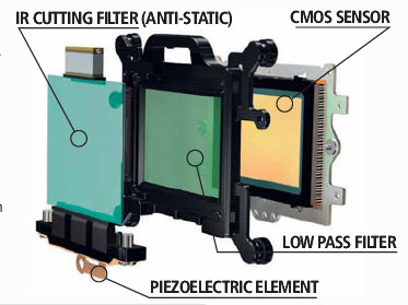

Fig. 1: An Image Representing use of CMOS Technology in Various Applications
CMOS technology has been adopted to design sensors, especially in the field of imaging. Due to the wide usage of CMOS based image sensors, CMOS sensors are often considered to be a synonym of CMOS based image sensors and have emerged as a competitor to CCD based image sensors.
Until recently, Charge Coupled Devices (CCDs) dominated most of the image sensing systems, i.e., cameras, camcorders, etc. CCDs have been in use in astronomical cameras, video camcorders and scanners. However of late, CMOS Imaging have emerged as an alternative to CCD imagers and it also offers better features.
Subsequent sections will discuss both CCD and CMOS sensor based imagers, their pros and cons, and also their applications. Further, other applications of CMOS technology in the field of sensing will be discussed.
CMOS Vs CCD
Invention of CCD marked the end of vacuum tube imagers used in television cameras as it overcame the disadvantages of vacuum tubes like chronic picture artifacts as lag and burn-in, fragility of large glass tubes or the sensitivity to shock, vibration and electromagnetic radiation, painstaking periodic alignment of tubes, etc. It also marked the beginning of a new era in imaging systems and for decades, it enjoyed quality advantages over the rival CMOS sensors. Wherever image quality was paramount, CCDs were preferred, CMOS were used mainly in applications where small size and low power were prime requirements.
With the technological development in CMOS technology, gap between CCD and CMOS sensors has narrowed; CMOS sensors can also achieve competitive quality. Choice amongst CCD and CMOS sensors has become increasingly difficult.
Both CCD and CMOS image sensors use large arrays of thousands (sometimes millions) of photo-sites, commonly called pixels. Both carry out same steps.
1. Light-to-charge conversion
Incident light is directed by the microlens (a tiny lens placed over the pixel to increase its effective size and thereby fill factor) onto the photo-sensitive area of each pixel where it is converted into electrons that collect in a semiconductor “bucket.”

Fig. 2: A Figure Illustrating Light-to-Charge Conversion
The bigger the pixel, the more light it can collect. Thus, big pixel sensors work best under low-light conditions. For the same number of pixels, bigger pixels results in bigger chip, this means higher cost. Conversely, smaller pixels enable smaller chip sizes and lower chip prices, as well as lower lens costs. But there are limitations on pixel size reduction. Smaller pixels are less sensitive to light, the optics required to resolve the pixels becomes expensive and requires expensive fabrication possesses.
2. Charge accumulation
As more light enters, more electrons accumulate into the bucket.
3. Transfer
Accumulated charge must be transferred to the signal conditioning and processing circuitry.
4. Charge-to-voltage conversion
The accumulated charge must be output as the voltage signal.
5. Amplification
Voltage signal is then amplified before it is fed to the camera circuitry.
Both CMOS and CCD perform all these tasks; however the aspect in which they differ is the order of execution of these tasks.
Brief on CCD Technology
BRIEF ON CCD TECHNOLOGY
CCDs were first invented in 1969 as a way to store data using bubble memory. In 1974, the first imaging CCD was produced by Fairchild Electronics with a format of 100×100 pixels.
CCD imager consists of two main parts: color filter and pixel array
• Color filter
Micro-lenses funnel light onto the photo-sensitive part of each pixel. On their way, the photons pass through a color filter array. The mosaic of these tiny filters captures color information. Color filters enable separate measurement of the red (R), green (G) and blue (B) photons. Color filter filters out wavelengths of unwanted colors and allows only specific colors of light to pass through a pixel sensor. For this purpose, each pixel is covered with a red, green and a blue filter according to a specific pattern, like the Bayer CFA pattern.

Fig. 3: A Figure Demonstrating Sub-Mosaic Pattern of Bayer CFA
Bayer filter uses the sub-mosaic 2x 2 patterns with one red, one blue and two green filters. As human’s eye has greater sensitivity for green light, two green filters are used.
• Pixel Array
The pixel array functions on the principle of the photoelectric effect and pixel sensors are responsible for capturing the intensity of the light passing through. The light intensity data is combined before being converted into an analog voltage signal, which is outputted to an external circuit board to be further processed.
After conversion of incident light into electrons, electron charge is accumulated in the same way as bucket stores water. The pixel charges are read using vertical and horizontal shift registers which act as charge carriers.
How CMOS Sensors work
CMOS SENSORS
A typical CMOS is an integrated circuit with an array of pixel sensors. In contrast to CCD, each pixel sensor in CMOS sensors contains its own light sensor, an amplifier and a pixel select switch. An analog-to-digital converter and other components critical to the operation of the pixel sensors are located on the CMOS sensor.
The CMOS sensor contains four main parts: the color filters, the pixel array, the digital controller, and the analog to digital convertor.

Fig. 4: A Figure Showing Parts of a CMOS Sensor
• Color Filter
Color filter is the same as was described in CCD based imager.
• Pixel Array
As in the case of CCD, function of the pixel array is to capture the intensity of the light passing through. Each pixel sensor converts the sensitivity of the incoming light to the voltage signal which is then fed to ADC for further processing
There are two types of architectures of Pixel sensors: Passive Pixel Sensor (PPS) & Active Pixel Sensors (APS).
Fig. 5: A Diagram Showing Passive Pixel Sensor Architecture of Pixel Sensors
In Passive Pixel sensors, only one photo-detector (without any local amplifier) per pixel is used, whereas in Active Pixel sensors, 3-4 transistors per pixel are used.
Fig. 6: A diagram Showing Active Pixel Sensor Architecture of Pixel Sensors
Passive Pixel sensors have smaller pixels and large fill factor but they are slow and have low SNR. On the other hand, active pixel sensors are fast, have good SNRs but larger pixels and low fill factor.
However, due to advancement of CMOS technology down to nm, pixel size/fill factor is no longer a big issue and APS is the technology which is preferred and used in most devices.
• ADC
The ADC takes the analog voltage signals from the pixel sensor array and converts them into a digital signal.
• Digital Controller
The digital controller governs the functioning of the the CMOS sensor; it controls the pixel array, ensures synchronism between all pixels, etc.
Operation of CMOS Sensors
Operation of CMOS Sensors
a) Pixel sensor acts like a charge bucket; accumulates electron charges the same way as water bucket stores water
b) Charge is converted to voltage & amplified at the pixel.
c) Individual CMOS microwire carry voltage from one pixel at a time, controlled by the pixel select switch
d) To output video signal, following steps are followed
1. All pixel select switches are turned ON. This outputs voltage of each pixel to column circuit.
2. Column select switches are turned ON from left to right. In this way, signal voltages of each pixel in the same row are output in order.
3. This is repeated for all rows from the top to the bottom in order, signal voltages of all pixels can be output from the top-left corner to the bottom-right corner of the image sensor.
e) These signal voltages are output to the signal processor of the camera.

Fig. 7: A Diagram Showing Operation of CMOS Sensor
CMOS SENSOR TYPES
Difference between types of CMOS sensors is generally due to the number of transistors (affecting fill factor) that are present for each pixel. A portion of the pixel sensor that is actually sensitive to light is called fill factor.
a) Rolling Shutter type
This has got limited number of transistors and therefore has a high fill factor. However, lines of pixels are exposed at different times and therefore, movement in the target gives a distorted image.
b) Global Shutter type
The number of transistors is high in this case resulting in a low fill factor. But, all the pixels are exposed at a time and thus the movement artifacts associated with rolling shutter type sensors are removed.
CCD & CMOS: Pros and Cons
CCD AND CMOS SENSORS: PROS AND CONS
1. Fabrication Process
CCD sensors use specialized fabrication that uses dedicated and costly manufacturing processes, whereas CMOS sensors rely on standard CMOS technology (used for IC fabrication like microprocessors, memory, etc.). As CMOS sensors can also integrate required electronics on the same chip, CMOS sensors results in compact and cost effective system
2. Dynamic Range
Dynamic range of CCD is roughly twice as that of CMOS sensor. This implies that if better colour depth is required, CCDs are likely to offer better results. On the other hand, CMOS are marginally more photosensitive.
3. Power Consumption
CMOS cameras have lower power consumption than CCDs but other CMOS circuitry may require more power. Low end CMOS sensors have low power requirements, but high speed CMOS cameras typically require more power than CCDs.
4. Noise
Two types of noise affect sensors’ performance: Temporal Noise and Fixed pattern noise. Fixed pattern Noise is more in CMOS, compared to CCDs because charge is converted to voltage at each pixel as compared to single point charge-voltage conversion in CCDs. In terms of temporal noise, CMOS sensors are better as the bandwidth of amplifiers at each pixel is lower than the output amplifier in case of CCD.
5. Image Quality
Due to poor fill factor of CMOS, photosensitivity of CMOS sensors is poor in low light conditions.
6. Uniformity of response
CCDs use single amplifier for all pixels and CMOS use separate amplifiers for each pixel. Pixel-to-pixel amplification differences lead to non-uniformity. Response of CCDs is pretty uniform.
7. Speed
CMOS sensors have higher speed due to the fact that it uses active pixels and ADCs on same chip leading to lesser propagation delays.
8. Readout area
CMOS sensors allow any region or even multiple regions to be read off the sensor. CCDs are limited by vertical scan read out
9. Smart functions
With the integration of signal processing circuitry on the CMOS sensor chip, functions like auto gain control, auto exposure control etc., anti-jitter, image compression, color encoding, motion tracking, etc. can be incorporated on-chip.
10. Overexposure effect
Overexposure can cause smearing around over-exposed pixels. Smearing is caused by spilling of charge into the shift register. Due to absence of shift registers in CMOS sensors, they are immune to this effect.
Various CMOS Sensors
OTHER CMOS SENSORS
• CMOS Humidity & Temperature Sensors
Swiss-based Sensirion AG has introduced an integrated, digital humidity and temperature sensors using CMOS “micro-machined” chip technology. SHT11 is a single chip RH and temperature sensing module with a calibrated digital output fabricated 

Fig. 8: A Representational Image of CMOS Humidity and Temperature Sensor
using CMOS technology.
Conventional humidity sensors determine relative air humidity using capacitive technology. However they suffer from poor long-term stability and complicated calibration. In addition, they require additional circuitry to convert analogue output to be interfaced with microprocessors, etc.
SHT11 uses a micro-machined finger electrode system with protective and polymer cover layers forming the capacitance for the sensor chip as well as simultaneously protecting the sensor from interference. The sensor chip can be interfaced directly to any microprocessor system by means of the digital 2-wire interface.
As the temperature sensor and the humidity sensor are integrated in a single unit, it removes measurement errors due to temperature gradients between the two sensing elements. The sensor offers high noise immunity, good stability, short response times, high precision, low power consumption, and has a small footprint
• 3D Imaging Sensor
DepthSense™ sensor is a patented CMOS chip from SoftKinetic DepthSense for 3D Imaging. It uses time-of-flight principle and provides a direct way for acquiring 3D information of objects enabling new applications such as gesture recognition. Such sensors are being integrated in cameras.
KODAK 9000 3D Panoramic System is another 3D imaging system for dental applications. With an impressive focused-field 3D, it can generate different types of facial images.
• CMOS X-ray Detectors
Flat panel CMOS X-ray detectors from Dexela are based on innovative crystalline Silicon based CMOS sensor design offering unprecedented speed and superior image quality. The detectors are suitable for a range of applications including mammography and tomosynthesis, angiographic imaging, bone densitometry, dental CBCT, scientific instrumentation and NDTs.
The major advantages of the technology are: high frame-rate, low noise, high reliability, absence of image lag and high spatial resolution. The clinical benefits are lower radiation dose to the patient combined with superior image quality when compared with flat panels based on amorphous Silicon sensor technology. Dexela uses the flexibility, speed and low noise of CMOS technology to create detectors that are flexible, faster, more sensitive, higher resolution and more stable than TFT based flat panel detectors
The main components of this detector are: CMOS image sensor, scintillator, control electronics, readout electronics and communications devices.
• CMOS Microhotplates
Cambridge CMOS Sensors provides innovative MEMS high temperature microhotplate technology for gas sensing, flow sensing and lab-on-a-chip applications. Technology uses standard CMOS process that enables high volume, low cost and low power sensor-on-a-chip solutions
• CMOS sensor for fluid flow
Burkert Fluid Control Systems uses CMOS technology for mass flow rate measurement of the gas by measuring the temperature differential.
It uses a Si chip in one place with an exposed diaphragm on the walls of the flow channel. A resistor is connected to the diaphragm; two temperature sensors are installed at upstream and downstream of it.
If the heating resistor is supplied with an excitation voltage, the voltage differential of the temperature sensors provides mass flow of the gas flowing through the channel.
You may also like:
Filed Under: Sensors, Tech Articles, Tutorials





Questions related to this article?
👉Ask and discuss on Electro-Tech-Online.com and EDAboard.com forums.
Tell Us What You Think!!
You must be logged in to post a comment.