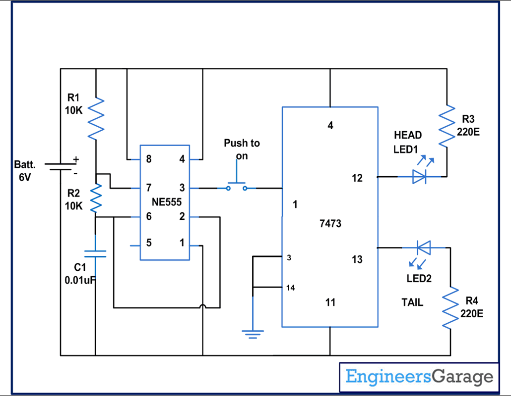
In this project 555 timer is wired in astable mode. 7473 IC contains two independent positive pulse triggered J-K flip-flops with complementary outputs.
The pin2 of the IC is for trigger input. When the voltage supplied to pin2 is less than 1/3 of the supply voltage, the output of the lower comparator forces the flip flop to have low logic state. This means output stage has reversing action. In other words, we can say that when output of the flip flop is LOW, the 555 timer’s output goes HIGH. Now if the power supply is first connected to astable circuit then initially the timing capacitor C1 is discharged. The voltage at pin2 becomes 0V and the output of timer is driven HIGH. Now C1 starts charging through R1 and R2. Capacitor C1 is also connected to pin6 which is threshold input of the timer.
Circuit Diagrams
Project Components
Filed Under: Electronic Projects


Questions related to this article?
👉Ask and discuss on EDAboard.com and Electro-Tech-Online.com forums.
Tell Us What You Think!!
You must be logged in to post a comment.