NXP Semiconductors recently announced the expansion of its LPC552x Microcontroller (MCU) family. With an enhanced working efficiency, the LPC5500 MCU series comes with some significant advantages for designers and developers.
 The list of added benefits includes peripheral and pin-software compatibility. These new MCUs use the 40-nm NVM process technology to accelerate time to market, power efficiency, and cost-effectiveness of final products.
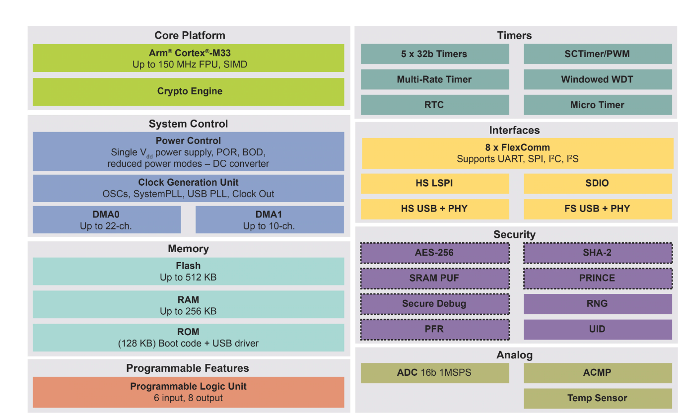
The LPC552x/S2x family is the star of LPC5500 series, it offers an optimum balance between performance, security, system integration, and efficiency for industrial IoT and general embedded devices.
The LPC5500 series family is a combination of high-performance efficacy of Cortex-M33 along with several high-speed interfaces, rich analogue integration, and an integrated power management IC.
Noteworthy features
- Can be availed in HTQFP64, VFBGA98, and HLQFP100 packaging.
- The operating temperature range goes from -40°C to 105°C.
- Voltage range 1.8-3.6 Volts.
- Power saving mode available.
- Programmable logic unit.
- USB FS, USB HS, and FlexComm.
- Cortex-M33 up to 150MHz along with MPU and FPU.
- Higher-level security, CASPER for hardware acceleration, PRINCE module for some real-time encryption, SRAM PUF, and AES-256 SHA2 module.
- On-chip flash from 256KB and up to 256KB SRAM.
- 16-bit ADC with five differential pairs of channels, temperature sensor, and ACMP.
- 5 x 32b Timers, WWDT, MRT, RTC, SC Timer/PWM.
The product series can be availed from NXP as well as its distribution partners for a resale price beginning from $1.63 for 10, 000-units. NXP also plans to accompany silicon release with LPC55S28-based evaluation kit for a resale of $39 (USD). Third-party support can be obtained from broad Arm ecosystem.
Filed Under: Components, News

Questions related to this article?
👉Ask and discuss on Electro-Tech-Online.com and EDAboard.com forums.
Tell Us What You Think!!
You must be logged in to post a comment.