Engineers Garage

  • Electronic Projects & Tutorials
    • Electronic Projects
      • Arduino Projects
      • AVR
      • Raspberry pi
      • ESP8266
      • BeagleBone
      • 8051 Microcontroller
      • ARM
      • PIC Microcontroller
      • STM32
    • Tutorials
      • Audio Electronics
      • Battery Management
      • Brainwave
      • Electric Vehicles
      • EMI/EMC/RFI
      • Hardware Filters
      • IoT tutorials
      • Power Tutorials
      • Python
      • Sensors
      • USB
      • VHDL
    • Circuit Design
    • Project Videos
    • Components
  • Articles
    • Tech Articles
    • Insight
    • Invention Stories
    • How to
    • What Is
  • News
    • Electronic Product News
    • Business News
    • Company/Start-up News
    • DIY Reviews
    • Guest Post
  • Forums
    • EDABoard.com
    • Electro-Tech-Online
    • EG Forum Archive
  • DigiKey Store
    • Cables, Wires
    • Connectors, Interconnect
    • Discrete
    • Electromechanical
    • Embedded Computers
    • Enclosures, Hardware, Office
    • Integrated Circuits (ICs)
    • Isolators
    • LED/Optoelectronics
    • Passive
    • Power, Circuit Protection
    • Programmers
    • RF, Wireless
    • Semiconductors
    • Sensors, Transducers
    • Test Products
    • Tools
  • Learn
    • eBooks/Tech Tips
    • Design Guides
    • Learning Center
    • Tech Toolboxes
    • Webinars & Digital Events
  • Resources
    • Digital Issues
    • EE Training Days
    • LEAP Awards
    • Podcasts
    • Webinars / Digital Events
    • White Papers
    • Engineering Diversity & Inclusion
    • DesignFast
  • Guest Post Guidelines
  • Advertise
  • Subscribe

Creating and Checking Gerber file using Eagle

By Anjali Sethiya July 7, 2013


Different kinds of PCB design software’s are available in market and according the requirement different users used different software. Like I am comfortable in designing my PCB on Eagle and my vendors who fabricate the PCB does not have Eagle than what will happen?

Hence to bridge the gap between the PCB designer and manufacture we use gerber file. Gerber file contain information about the PCB like what will be the pad size, drill size, name of component etc. With the help of gerber file information obtained and manufacture feed the data into their machinery to manufacture PCB. The most common format that is used today is RS-274-X. But before using always check with the board manufacture.

Steps for creating Gerber-

1. First of all check your board properly for any errors or warning. Because once you have given the board for manufacturing than you cannot make changes so be careful.

2. Open your finish board. Then click on File and then on CAM Processor.

Creating and Checking Gerber File using Eagle


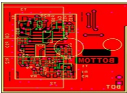
3. When you click on CAM Processor following window will appear.

Creating and Checking Gerber File using Eagle

4. Now click on File than open then job. Following window will appear.

Creating and Checking Gerber File using Eagle

5. When you select Job following widow will appear.

Creating and Checking Gerber File using Eagle

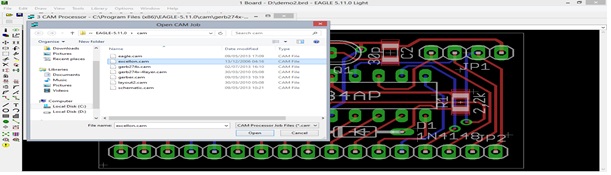
6. Now select Gerber274*.cam.

For a 2 layer board with silkscreen and solder mask on both sides so number of layer created will be seven and if you are designing 4 layer board then select gerber274*.4layer.cam.  So take care for number of layers.

7. Now again go to File than Open than click on Job and select excellon.cam .Following window will appear.

Creating and Checking Gerber File using Eagle

8. Then click on Ok. Following window will appear.

9. Now click on Process job. This will generate drill data.

Creating and Checking Gerber File using Eagle

10. Now similarly click on File then Open then Job and select one by one all. Like eagle.com then Open than Process Job. Do similarly for gerber.cam, layout2.cam etc.

If you want to see the gerber data, open the file on word pad like I have opened the data of demo.cmp. Demo is the name of my file and .cmp indicates that it is the data of top layer. Your data will somewhat look like as shown (this is not the full data I have cut short it)-

Similarly you can also see another files data but it is not possible for us to read this data.  And this data are fed to machine for manufacturing of PCB. 

 How to See Gerber Data

How you can see your gerber data 

If you want to see your gerber file then you have to first download a software name gerber viewer and install it on your computer. It is freely available software. It is a good practise to check your layout before manufacturing because once it has been fabricated you cannot correct your mistake. Or it may happen that PCB will not be of any use this will lead to wastage of time and money both. So check it correctly. Once software is installed it will look like-

Creating and Checking Gerber File using Eagle

Now first of all find the location where you have saved all your file like I have saved it in D drive. You should always save all gerber file data on same location.

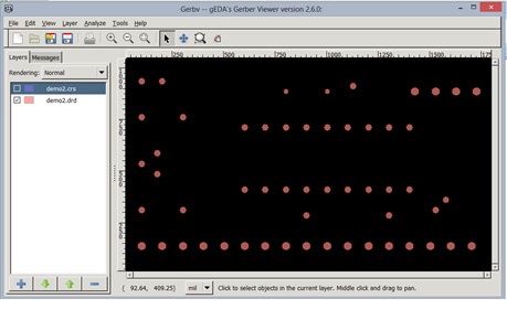
Then in the software select File than Open layer. Following window will appear and it will allow you to browse your location of gerber file. 

Creating and Checking Gerber File using Eagle

Then I have selected the file demo2.drd. Here demo is the same file which are use to generate gerber and .drd show the holes to be drilled so you can verify the same from your layout as shown in figure below.

Creating and Checking Gerber File using Eagle

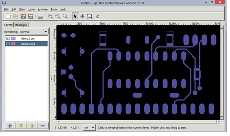
Similarly go to File then Open layer then select demo2.crs and you get pad also as shown in figure. 

Creating and Checking Gerber File using Eagle

Similarly you can check different layers.  Points to Remember 

Points to remember while making Gerber file
Before sending your data to manufacturer you should organise your data so that it will easy for the vendor to make the layout from it. You should keep this simple rule in your mind before placing an order to resolve PCB design issue.
Rule 1
You should always organise your data in folder like make folder for-
1. Drill data which will contain information about drill size, number of drill holes, pad size.
2. Top layer which contains information about component footprint, pads and vias.
3. Bottom layer which contains information about track connection pads and vias.
Similarly make folders for top solder mask, bottom silk screen, and top silk screen.
Rule 2
Do not compress or enlarge your PCB before making the Gerber file. Always provide 1:1 data. So that after manufacturing, you will receive the same size PCB which you have design. Otherwise if you have design to fit into a particular board then it will create a problem and this bad practice of PCB designing.
Rule 3
Take care of your Gerber file that it does not contain apertures with zero size. Unit of measurement of aperture is mm or inch. Aperture represents the shapes and size of each element on PCB like of pads and track. These are also known as D-code list.
Rule 4
Take care your Gerber file does not contain Exelon data with zero size. This also measure in mm and inches. Exelon file give information about holes size and where to drill the hole.
Rule 5
Always use same offset for all Gerber layer and Exelon drill layer.
Rule 6
While designing PCB always used same unit may be mm or inches. Like if you are using mm for resistor pads than use same unit for other component present on PCB. Because during conversion (mm to inch or inch to mm) it may possible hole size or pad may reduce or become more. And it will create problem while mounting the component.
Rule 7
Try to use same grid for your Gerber and Exelon data which allow perfect match. While drawing PCB on Eagle software always try to use grid size as 0.1 inches in multiple of one.
Rule 8
Do not make Gerber of mirror PCB. Always make Gerber of each layer as you have make one is to one.  Make sure that data you are going to manufacture is seen from top to bottom through the PCB.
Rule 9
If you are naming component on top side than do not mirror it  should be in readable format, but when you are using it in bottom side like indicating name of company etc then mirror it.
Top layer
           TOP LAYER                                                     BOTTOM LAYER
Rule 10
If you have to use the same PCB again than it is good practise to indicate some identification number. So that it will become easy for the manufacture and you to give the order again. 


Project Source Code


Project Source Code

###


%!PS-Adobe-3.0 EPSF-3.0

%%Title: EAGLE Drawing D:/demo2.brd

%%Creator: EAGLE

%%Pages: 1

%%BoundingBox: 0 0 132 75

%%EndComments


% Coordinate transfer:


/EU { 254 div 0.072 mul } def

/inch { 72 mul } def


% Linestyle:


1 setlinecap

1 setlinejoin


% Drawing functions:


/l {  % draw a line

   /lw exch def

   /y2 exch def

   /x2 exch def

   /y1 exch def

   /x1 exch def

   newpath

   x1 EU y1 EU moveto

   x2 EU y2 EU lineto

   lw EU setlinewidth

   stroke

   } def


/h {  % draw a hole

   /d  exch def

   /y  exch def

   /x  exch def

   d 0 gt {

     newpath

     x EU y EU d 2 div EU 0 360 arc

     currentgray dup

     1 exch sub setgray

     fill

     setgray

     } if

   } def


/edge { 0.20710678119 mul } def


/o {  % draw an octagon

   /an exch def

   /dy exch def

   /dx exch def

   /y  exch def

   /x  exch def

   gsave

   x EU y EU translate

   an dx dy lt { 90 add /dx dy /dy dx def def } if rotate

   newpath

      0 dx 2 div sub EU                    0 dy edge  add EU moveto

      0 dx dy sub 2 div sub dy edge sub EU 0 dy 2 div add EU lineto

      0 dx dy sub 2 div add dy edge add EU 0 dy 2 div add EU lineto

      0 dx 2 div add EU                    0 dy edge  add EU lineto

      0 dx 2 div add EU                    0 dy edge  sub EU lineto

      0 dx dy sub 2 div add dy edge add EU 0 dy 2 div sub EU lineto

      0 dx dy sub 2 div sub dy edge sub EU 0 dy 2 div sub EU lineto

      0 dx 2 div sub EU                    0 dy edge  sub EU lineto

   closepath

   fill

   grestore

   } def


2724 2660 462974 2660 0 l

462974 2660 462974 262910 0 l

462974 262910 2724 262910 0 l

2724 262910 2724 2660 0 l

255074 230448 255074 219272 11176 l

204274 230448 204274 219272 11176 l

26474 78810 13208 13208 180.0 o

77274 78810 13208 p

26474 193110 13208 13208 180.0 o

77274 193110 13208 p

223070 72460 236278 72460 13208 l

324670 72460 337878 72460 13208 l

153474 97606 153474 110814 13208 l

178874 97606 178874 110814 13208 l

204274 97606 204274 110814 13208 l

229674 97606 229674 110814 13208 l

255074 97606 255074 110814 13208 l


###


Filed Under: Electronic Projects
Tagged With: eagle, gerber file
 

Next Article

← Previous Article
Next Article →

Questions related to this article?
👉Ask and discuss on Electro-Tech-Online.com and EDAboard.com forums.


Tell Us What You Think!! Cancel reply

You must be logged in to post a comment.

EE TECH TOOLBOX

“ee
Tech Toolbox: 5G Technology
This Tech Toolbox covers the basics of 5G technology plus a story about how engineers designed and built a prototype DSL router mostly from old cellphone parts. Download this first 5G/wired/wireless communications Tech Toolbox to learn more!

EE Learning Center

EE Learning Center
“engineers
EXPAND YOUR KNOWLEDGE AND STAY CONNECTED
Get the latest info on technologies, tools and strategies for EE professionals.

HAVE A QUESTION?

Have a technical question about an article or other engineering questions? Check out our engineering forums EDABoard.com and Electro-Tech-Online.com where you can get those questions asked and answered by your peers!


RSS EDABOARD.com Discussions

  • IGBTs without negative gate drive
  • How to generate and use large‑signal S‑parameter (LSSP) files for PA harmonic‑balance (HB) simulations?
  • VHF radio
  • High failure rate of LLC converter
  • Broad band impedance matching network for loop antenna using transformer for wireless power transfer

RSS Electro-Tech-Online.com Discussions

  • More fun with ws2812 this time XC8 and CLC
  • Pickit 5
  • Pic18f25q10 osccon1 settings swordfish basic
  • turbo jet fan - feedback appreciated.
  • I Wanna build a robot

Featured – LoRa/LoRaWan Series

  • What is the LoRaWAN network and how does it work?
  • Understanding LoRa architecture: nodes, gateways, and servers
  • Revolutionizing RF: LoRa applications and advantages
  • How to build a LoRa gateway using Raspberry Pi
  • How LoRa enables long-range communication
  • How communication works between two LoRa end-node devices

Recent Articles

  • How IoT network topologies work
  • The top five AI startups to watch in 2025
  • STMicroelectronics unveils SoC based on secure MCU
  • Nexperia’s 48 V ESD diodes support higher data rates with ultra-low capacitance design
  • Taoglas releases Patriot antenna with 18 integrated elements covering 600 to 6000 MHz

EE ENGINEERING TRAINING DAYS

engineering

Submit a Guest Post

submit a guest post
Engineers Garage
  • Analog IC TIps
  • Connector Tips
  • Battery Power Tips
  • DesignFast
  • EDABoard Forums
  • EE World Online
  • Electro-Tech-Online Forums
  • EV Engineering
  • Microcontroller Tips
  • Power Electronic Tips
  • Sensor Tips
  • Test and Measurement Tips
  • 5G Technology World
  • Subscribe to our newsletter
  • About Us
  • Contact Us
  • Advertise

Copyright © 2025 WTWH Media LLC. All Rights Reserved. The material on this site may not be reproduced, distributed, transmitted, cached or otherwise used, except with the prior written permission of WTWH Media
Privacy Policy

Search Engineers Garage

  • Electronic Projects & Tutorials
    • Electronic Projects
      • Arduino Projects
      • AVR
      • Raspberry pi
      • ESP8266
      • BeagleBone
      • 8051 Microcontroller
      • ARM
      • PIC Microcontroller
      • STM32
    • Tutorials
      • Audio Electronics
      • Battery Management
      • Brainwave
      • Electric Vehicles
      • EMI/EMC/RFI
      • Hardware Filters
      • IoT tutorials
      • Power Tutorials
      • Python
      • Sensors
      • USB
      • VHDL
    • Circuit Design
    • Project Videos
    • Components
  • Articles
    • Tech Articles
    • Insight
    • Invention Stories
    • How to
    • What Is
  • News
    • Electronic Product News
    • Business News
    • Company/Start-up News
    • DIY Reviews
    • Guest Post
  • Forums
    • EDABoard.com
    • Electro-Tech-Online
    • EG Forum Archive
  • DigiKey Store
    • Cables, Wires
    • Connectors, Interconnect
    • Discrete
    • Electromechanical
    • Embedded Computers
    • Enclosures, Hardware, Office
    • Integrated Circuits (ICs)
    • Isolators
    • LED/Optoelectronics
    • Passive
    • Power, Circuit Protection
    • Programmers
    • RF, Wireless
    • Semiconductors
    • Sensors, Transducers
    • Test Products
    • Tools
  • Learn
    • eBooks/Tech Tips
    • Design Guides
    • Learning Center
    • Tech Toolboxes
    • Webinars & Digital Events
  • Resources
    • Digital Issues
    • EE Training Days
    • LEAP Awards
    • Podcasts
    • Webinars / Digital Events
    • White Papers
    • Engineering Diversity & Inclusion
    • DesignFast
  • Guest Post Guidelines
  • Advertise
  • Subscribe