This tutorial will teach you how to use the inbuilt DAC of LPC1768 to generate a analog output (cosine wave) from a digital pin and display in the CRO. For setting up the Environment for the development of ARM cortex M3 is well discussed in this article.
The LPC 1768 is ARM Cortex- M3 based Microcontrollers for embedded application features in low power consumption and a high level of integration. The ARM Cortex M3 is designed in a such way to enhance debug features and a higher level of system integration. It clocks at a CPU frequency of 100 MHz, and incorporates a 3-stage pipeline and uses a Harvard architecture with separate local instruction and data buses for third bus peripherals. The ARM Cortex- M3 CPU have an internal pre-fetch unit to support speculative branching. The peripheral components include 512KB of flash memory, 64kb of data memory, Ethernet MAC, USB OTG, 4 UART’s, 8-channel general purpose DMA controller, 2 SSP Controllers, 10-bit DAC, Quadrature encoder interface, SPI interface, 3 I2C bus interface, 2 input plus 2 outputs I2S bus interface, 4 general purpose timers, ultra-low power Real-Time Clock (RTC) with separate battery supply, and up to 70 general purpose I/O pins, 6-output general purpose PWM. The LPC1768/66/65/64 are pin-compatible with the 100-pin LPC236x ARM7-based Microcontroller series.

Fig. 1: DAC Programming In LPC1768 Prototype
The ARM Cortex M3(NXP LPC1768) contains a 10-bit DAC (Digital to Analog Converter). All the pins of LPC1768 has alternate functions to the default digital input-output functions we have to first select the pin for the appropriate function. ADC of it has 8 multiplexed pins. (See table below). The second alternate function for P0.26 (pin 6) is AOUT. ie the DAC output.
SELECTING CLOCK FOR DAC:
By assuming that the main clock for the LPC1768 has been programmed. Each LPC1768 peripheral including the DAC has a clock derived from the main clock as illustrated.
Peripheral Clock Divider
As shown in the below block the frequency of the peripheral clock is determined by two bits in the PCLKSEL registers. DAC is included in PCLKSEL0. With the NXP LPC1768 the peripheral clocks are always active. Following RESET PCLKSEL registers are cleared setting the peripheral clock frequency to CCLK/4 to all the peripherals. The user will have a choice of frequency which can be determined by two bits for each peripherals among the peripheral clock selection registers PCLKSEL0 and PCLKSEL1. By default at reset all values are 00 ie CCLK/4.
|
00 |
PCLK_peripheral = CCLK/4 |
|
01 |
PCLK_peripheral = CCLK |
|
10 |
PCLK_peripheral = CCLK/2 |
|
11 |
PCLK_peripheral = CCLK/8, except for CAN1, CAN2, |
Fig. 2: Bit Value Of PCLK_Peripheral For Clock Frequency
|
Bit |
Symbol |
Description |
|
1:0 |
PCLK_WDT |
Peripheral clock selection for WDT. |
|
3:2 |
PCLK_TIMER0 |
Peripheral clock selection for TIMER0. |
|
5:4 |
PCLK_TIMER1 |
Peripheral clock selection for TIMER1. |
|
7:6 |
PCLK_UART0 |
Peripheral clock selection for UART0. |
|
9:8 |
PCLK_UART1 |
Peripheral clock selection for UART1. |
|
11:10 |
– |
Reserved. |
|
13:12 |
PCLK_PWM1 |
Peripheral clock selection for PWM1. |
|
15:14 |
PCLK_I2C0 |
Peripheral clock selection for I2C0. |
|
17:16 |
PCLK_SPI |
Peripheral clock selection for SPI. |
|
19:18 |
– |
Reserved. |
|
21:20 |
PCLK_SSP1 |
Peripheral clock selection for SSP1. |
|
23:22 |
PCLK_DAC |
Peripheral clock selection for DAC. |
|
25:24 |
PCLK_ADC |
Peripheral clock selection for ADC. |
|
27:26 |
PCLK_CAN1 |
Peripheral clock selection for CAN1.[1] |
|
29:28 |
PCLK_CAN2 |
Peripheral clock selection for CAN2.[1] |
|
31:30 |
PCLK_ACF |
Peripheral clock selection for CAN acceptance filtering.[1] |
Fig. 3: Bit Value And Description Of PCLK_Peripheral In LPC1768
Code snipet:
LPC_SC->PCLKSEL0 |= 1 <<24; //pclk = cclk
SELECTING THE DAC FUNCTION TO GPIO:
As we discussed in the previous articles the GPIO function is selected with the help of PINSEL register of the Pin control block. Port 1 is controlled by PINSEL0,1 and Port 1 is controlled by PINSEL2,3. RESET makes all the bits of PINSEL to be cleared results in attachment of GPIO function to the pins.
Each pin is controlled by 2 consecutive bits of PINSEL register. PINSEL0[1:0] bits controls the Pin P0.0, PINSEL0[3:2] bits controls the Pin P0.1. PINSEL0[31:30] bits controls the Pin P0.15, etc.- PSEL3[31:30] bits will control the pins Pin P1.31. The DAC is attached to pin P0.26. The following code will select alternate function 2 (DAC or AOUT) for pin P0.26.
|
Adc Channel |
Port Pin |
Pin Functions |
Associated PINSEL Register |
|
AD0 |
P0.23 |
0-GPIO, 1-AD0[0], 2-I2SRX_CLK, 3-CAP3[0] |
14,15 bits of PINSEL1 |
|
AD1 |
P0.24 |
0-GPIO, 1-AD0[1], 2-I2SRX_WS, 3-CAP3[1] |
16,17 bits of PINSEL1 |
|
AD2 |
P0.25 |
0-GPIO, 1-AD0[2], 2-I2SRX_SDA, 3-TXD3 |
18,19 bits of PINSEL1 |
|
AD3 |
P0.26 |
0-GPIO, 1-AD0[3], 2-AOUT, 3-RXD3 |
20,21 bits of PINSEL1 |
|
AD4 |
P1.30 |
0-GPIO, 1-VBUS, 2- , 3-AD0[4] |
28,29 bits of PINSEL3 |
|
AD5 |
P1.31 |
0-GPIO, 1-SCK1, 2- , 3-AD0[5] |
30,31 bits of PINSEL3 |
|
AD6 |
P0.3 |
0-GPIO, 1-RXD0, 2-AD0[6], 3- |
6,7 bits of PINSEL0 |
|
AD7 |
P0.2 |
0-GPIO, 1-TXD0, 2-AD0[7], 3- |
4,5 bits of PINSEL0 |
Fig. 4: Selecting DAC Function Using GPIO Pins With PINSEL register In LPC1768
Code snipet:
LPC_PINCON->PINSEL1 |= 0x02<<20; //Pin P0.26 allocated to alternate function 2
DAC Registers and DAC Operation:
For simple operations only the DAC converter register DACR is required.
DACR register:
|
Bit |
Symbol |
Description |
Reset Value |
|
5:0 |
– |
Reserved, user software should not write ones to reserved bits. |
NA |
|
15:6 |
VALUE |
After the selected settling time after this field is written with a newVALUE, the voltage on the AOUT pin (with respect to VSSA) is VALUE x ((VREFP – VREFN)/1024) + VREFN. |
0 |
|
16 |
BIAS[1] |
0 The settling time of the DAC is 1 us max, and the maximum current is 700 uA. |
0 |
|
31:17 |
– |
Reserved, user software should not write ones to reserved bits. |
|
Fig. 5: Bit Description Of DACR Register In LPC1768
The DACR register is a read/write register that includes the digital value to be converted to analog, and a bit that trades off performance vs. power. With references voltages between 3.3 and 0 the output AOUT will be;
AOUT = 3.3*VALUE/1024
Code for DAC to generate a 1Volt output.
Code snipet:
LPC_DAC->DACR = 0x155<<6; //output = 1 volt
Controlling the DAC ouput with the System Tick:
In this cosine example the time between steps can also be determined by the software delay loop. However a software loop will use most of the processors resources. A alternate better solution is to use a hardware timer such as the system tick to generate a time reference to control the output changes. The tick period is set by the register LOAD. The system tick will generate a non maskable interrupt which vectors to the routine SysTick_Handler( ) that generates an output voltage step.
Create a project using Keil uvision4 for LPC1768 Microcontroller:
In this section, we will start creating a project in Keil MDK we have already installed Keil µVision and Co-MDK Plug-in + CoLinkEx Drivers required for the CoLinkEx programming adapter. You can start by downloading the project files and kick start your practical experiment.
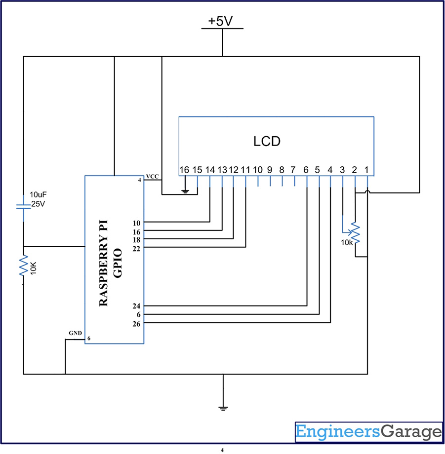
For more details on interfacing the LCD in 4 bit mode with LPC1768 refer this link.

Fig. 6: Output Waveform Of DAC Programming In LPC1768
Project Source Code
###The codes are linked in Description ###
Circuit Diagrams
Project Components
Project Video
Filed Under: ARM.
Filed Under: ARM.

Questions related to this article?
👉Ask and discuss on EDAboard.com and Electro-Tech-Online.com forums.
Tell Us What You Think!!
You must be logged in to post a comment.