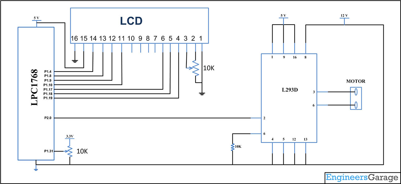
In this article we are going discuss about the interfacing of DC Motor to ARM Cortex M3 (LPC1768). We are going to code the LPC1768 in such a way that the speed of the DC motor is controlled by the potentiometer connected to the ADC input and the speed is also displayed on the LCD. For more details about ADC interface refer this article. For Setting up the Environment for the development of ARM cortex M3 go through this article. For detailed information about the ADC interface you can refer this article.

Fig. 1: DC Motor Control Using PWM Of LPC1768 Prototype
In most of the applications controlling the speed of DC motor is essential where the precision and protection are the essence. Here we will use the PWM technique to control the speed of the motor. For more details refer this article Speed control using PWM modulation.
LPC1768 has one PWM channel with six ports. PWM changes the average output voltage by fast switching. By changing the on time, the output voltage can be 0 to 100%. There are two software parameters that need a little explanation: cycle and offset. Cycle is the length of a PWM duty cycle and offset is the on time of a duty cycle.
For example: when the cycle time is 1000 and the offset:
0, the output voltage = 0%
255, the output voltage = 25.5%
1000, the output voltage = 100%
POWERING THE PWM:
PCON register bits description:
|
Bit |
Symbol |
Description |
Reset value |
|
0 |
– |
Reserved. |
NA |
|
1 |
PCTIM0 |
Timer/Counter 0 power/clock control bit. |
1 |
|
2 |
PCTIM1 |
Timer/Counter 1 power/clock control bit. |
1 |
|
3 |
PCUART0 |
UART0 power/clock control bit. |
1 |
|
4 |
PCUART1 |
UART1 power/clock control bit. |
1 |
|
5 |
– |
Reserved. |
NA |
|
6 |
PCPWM1 |
PWM1 power/clock control bit. |
1 |
|
7 |
PCI2C0 |
The I2C0 interface power/clock control bit. |
1 |
|
8 |
PCSPI |
The SPI interface power/clock control bit. |
1 |
|
9 |
PCRTC |
The RTC power/clock control bit. |
1 |
|
10 |
PCSSP1 |
The SSP 1 interface power/clock control bit. |
1 |
|
11 |
– |
Reserved. |
NA |
|
12 |
PCADC |
A/D converter (ADC) power/clock control bit. |
0 |
|
13 |
PCCAN1 |
CAN Controller 1 power/clock control bit. |
0 |
|
14 |
PCCAN2 |
CAN Controller 2 power/clock control bit. |
0 |
|
15 |
PCGPIO |
Power/clock control bit for IOCON, GPIO, and GPIO interrupts. |
1 |
|
16 |
PCRIT |
Repetitive Interrupt Timer power/clock control bit. |
0 |
|
17 |
PCMCPWM |
Motor Control PWM |
0 |
|
18 |
PCQEI |
Quadrature Encoder Interface power/clock control bit. |
0 |
|
19 |
PCI2C1 |
The I2C1 interface power/clock control bit. |
1 |
|
20 |
– |
Reserved. |
NA |
|
21 |
PCSSP0 |
The SSP0 interface power/clock control bit. |
1 |
|
22 |
PCTIM2 |
Timer 2 power/clock control bit. |
0 |
|
23 |
PCTIM3 |
Timer 3 power/clock control bit. |
0 |
|
24 |
PCUART2 |
UART 2 power/clock control bit. |
0 |
|
25 |
PCUART3 |
UART 3 power/clock control bit. |
0 |
|
26 |
PCI2C2 |
I2C interface 2 power/clock control bit. |
1 |
|
27 |
PCI2S |
I2S interface power/clock control bit. |
0 |
|
28 |
– |
Reserved. |
NA |
|
29 |
PCGPDMA |
GPDMA function power/clock control bit. |
0 |
|
30 |
PCENET |
Ethernet block power/clock control bit. |
0 |
|
31 |
PCUSB |
USB interface power/clock control bit. |
0 |
Fig. 2: Bit Description Of PCON Register In LPC1768
Following reset the PCPWM1 (Power Clock Control Bit to PWM1) bit is set and is enabled by default.
SELECTING CLOCK FOR ADC:
By assuming that the main clock for the LPC1768 has been programmed. Each LPC1768 peripheral including the PWM has a clock derived from the main clock as illustrated.
Peripheral Clock Divider
As shown in the below block the frequency of the peripheral clock is determined by two bits in the PCLKSEL registers. PWM is included in PCLKSEL0. With the NXP LPC1768 the peripheral clocks are always active. Following RESET PCLKSEL registers are cleared setting the peripheral clock frequency to CCLK/4 to all the peripherals. The user will have a choice of frequency which can be determined by two bits for each peripherals among the peripheral clock selection registers PCLKSEL0 and PCLKSEL1. By default at reset all values are 00 ie CCLK/4.
|
00 |
PCLK_peripheral = CCLK/4 |
|
01 |
PCLK_peripheral = CCLK |
|
10 |
PCLK_peripheral = CCLK/2 |
|
11 |
PCLK_peripheral = CCLK/8, except for CAN1, CAN2, |
Fig. 3: Bit Value Of PCLK_Peripheral For Clock Frequency
|
Bit |
Symbol |
Description |
|
1:0 |
PCLK_WDT |
Peripheral clock selection for WDT. |
|
3:2 |
PCLK_TIMER0 |
Peripheral clock selection for TIMER0. |
|
5:4 |
PCLK_TIMER1 |
Peripheral clock selection for TIMER1. |
|
7:6 |
PCLK_UART0 |
Peripheral clock selection for UART0. |
|
9:8 |
PCLK_UART1 |
Peripheral clock selection for UART1. |
|
11:10 |
– |
Reserved. |
|
13:12 |
PCLK_PWM1 |
Peripheral clock selection for PWM1. |
|
15:14 |
PCLK_I2C0 |
Peripheral clock selection for I2C0. |
|
17:16 |
PCLK_SPI |
Peripheral clock selection for SPI. |
|
19:18 |
– |
Reserved. |
|
21:20 |
PCLK_SSP1 |
Peripheral clock selection for SSP1. |
|
23:22 |
PCLK_DAC |
Peripheral clock selection for DAC. |
|
25:24 |
PCLK_ADC |
Peripheral clock selection for ADC. |
|
27:26 |
PCLK_CAN1 |
Peripheral clock selection for CAN1.[1] |
|
29:28 |
PCLK_CAN2 |
Peripheral clock selection for CAN2.[1] |
|
31:30 |
PCLK_ACF |
Peripheral clock selection for CAN acceptance filtering.[1] |
Fig. 4: Bit Value And Description Of PCLK_Peripheral Register In LPC1768
SELECTING THE PWM FUNCTION TO GPIO:
The block diagram below shows the PWM pins multiplexed with other GPIO pins. The PWM pin can be enabled by configuring the corresponding PINSEL register to select PWM function. When the PWM function is selected for that pin in the Pin Select register, other Digital signals are disconnected from the PWM input pins.
|
PWM Channel |
Port Pin |
Pin Functions |
Associated PINSEL Register |
|
PWM1.1 |
P2.0 |
0-GPIO, 1- PWM1.1, 2-TXD1, 3- |
1,0 bits of PINSEL4 |
|
PWM1.2 |
P2.1 |
0-GPIO, PWM1.2, 2-RXD1, 3- |
3,2 bits of PINSEL4 |
|
PWM1.3 |
P2.2 |
0-GPIO, PWM1.3, 2-CTS1, 3- |
5,4 bits of PINSEL4 |
|
PWM1.4 |
P2.3 |
0-GPIO, 1- PWM1.4, 2-DCD1, 3- |
7,6 bits of PINSEL4 |
|
PWM1.5 |
P2.4 |
0-GPIO, 1- PWM1.5, 2-DSR1 , 3- |
9,8 bits of PINSEL4 |
|
PWM1.6 |
P2.5 |
0-GPIO, 1- PWM1.6, 2-DTR1 , 3- |
11,10 bits of PINSEL4 |
Fig. 5: Configuring PWM Pins With PINSEL Register In LPC1768
Code snippet:
In the PWM library we are using a switch case to select the port according to the user input.
PWM REGISTERS:
The registers associated with LPC1768 ADC are
-
IR-> Interrupt Register: The IR can be written to clear interrupts. The IR can be read to identify which of eight possible interrupt sources are pending.
-
TCR-> Timer Control Register: The TCR is used to control the Timer Counter functions. The Timer Counter can be disabled or reset through the TCR.
-
PR- > Prescale Register: The TC is incremented every PR+1 cycles of PCLK.
-
MCR-> Match Control Register: The MCR is used to control if an interrupt is generated and if the TC is reset when a Match occurs.
-
MR0 – MR6-> Match Register: Each can be enabled in the MCR to reset the TC, stop both the TC and PC, and/or generate an interrupt when it matches the TC.
-
PCR-> PWM Control Register: Enables PWM outputs and selects PWM channel types as either single edge or double edge controlled.
-
LCR-> Load Enable Register: Enables use of new PWM match values.
PWM REGISTER CONFIGURATION:
IR (Interrupt Register)
The PWM Interrupt Register consists of 11 bits, 7 for the match interrupts and 4 reserved for the future use. If an interrupt is generated then the corresponding bit in the PWMIR will be high. Otherwise, the bit will be low. Writing logic 1 to the corresponding IR bit will reset the interrupt. Writing a 0 has no effect.
|
Bit |
Symbol |
Description |
Reset Value |
|
0 |
PWMMR0 Interrupt |
Interrupt flag for PWM match channel 0. |
0 |
|
1 |
PWMMR1 Interrupt |
Interrupt flag for PWM match channel 1. |
0 |
|
2 |
PWMMR2 Interrupt |
Interrupt flag for PWM match channel 2. |
0 |
|
3 |
PWMMR3 Interrupt |
Interrupt flag for PWM match channel 3. |
0 |
|
4 |
PWMCAP0 Interrupt |
Interrupt flag for capture input 0 |
0 |
|
5 |
PWMCAP1 Interrupt |
Interrupt flag for capture input 1. |
0 |
|
7:6 |
– |
Reserved, user software should not write ones to reserved bits. The value read from a reserved bit is not defined. |
NA |
|
8 |
PWMMR4 Interrupt |
Interrupt flag for PWM match channel 4. |
0 |
|
9 |
PWMMR5 Interrupt |
Interrupt flag for PWM match channel 5. |
0 |
|
10 |
PWMMR6 Interrupt |
Interrupt flag for PWM match channel 6. |
0 |
|
31:11 |
– |
Reserved, user software should not write ones to reserved bits. The value read from a reserved bit is not defined. |
NA |
Fig. 6: Bit Address Of PWM Interrupt Register In LPC1768
TCR (TIMER CONTROL REGISTER)
The PWM Timer Control Register (PWMTCR) is used to control the operation of the PWM Timer Counter.
|
Bit |
Symbol |
Description |
Reset Value |
|
0 |
Counter Enable |
1 ->The PWM Timer Counter and PWM Prescale Counter are enabled for counting. 0 ->The counters are disabled. |
0 |
|
1 |
Counter Reset |
1 ->The PWM Timer Counter and the PWM Prescale Counter are synchronously reset on the next positive edge of PCLK. The counters remain reset until this bit is returned to zero. 0 ->Clear reset. |
0 |
|
2 |
– |
Reserved, user software should not write ones to reserved bits. The value read from a reserved bit is not defined. |
NA |
|
3 |
PWM Enable |
1 ->PWM mode is enabled (counter resets to 1). PWM mode causes the shadow registers to operate in connection with the Match registers. A program write to a Match register will not have an effect on the Match result until the corresponding bit in PWMLER has been set, followed by the occurrence of a PWM Match 0 event. Note that the PWM Match register that determines the PWM rate (PWM Match Register 0 – MR0) must be set up prior to the PWM being enabled. Otherwise a Match event will not occur to cause shadow register contents to become effective. 0 ->Timer mode is enabled (counter resets to 0). |
0 |
|
31:4 |
– |
Reserved, user software should not write ones to reserved bits. The value read from a reserved bit is not defined. |
NA |
Fig. 7: Bit Value Of PWM Timer Control Register In LPC1768
Create a project using Keil uvision4 for LPC1768 Microcontroller:
In this section, we will start creating a project in Keil MDK we have already installed Keil µVision and Co-MDK Plug-in + CoLinkEx Drivers required for the CoLinkEx programming adapter. You can start by downloading the project files and kick start your practical experiment.
Code Description:
Here the Library PWM.C is used to configure all the PWM functions and ADC is used as per the previous tutorial.
PWM_Init( CHANNEL_NUM, cycle );
PWM_Set( CHANNEL_NUM, cycle, offset );
PWM_Start( CHANNEL_NUM );
These are the functions used for our application. Here CHANNEL NUM macro defines 1.
offset = adc_result/4;
The adc_result is divided by 4 to get the output from 0 to 1000 to the offset.
PWM_Set( CHANNEL_NUM, cycle, offset );
This is the function to set the PWM in the output pin.
For more details on interfacing the LCD in 4 bit mode with LPC1768 refer this link.
Project Source Code
###The codes are linked in Description ###
Circuit Diagrams
Project Components
Project Video
Filed Under: ARM.
Filed Under: ARM.

Questions related to this article?
👉Ask and discuss on EDAboard.com and Electro-Tech-Online.com forums.
Tell Us What You Think!!
You must be logged in to post a comment.