Many times, there is need to step up or step down DC voltages. The circuits for stepping up or stepping down DC voltages are not simple as is the case with AC voltages. The level changing of DC voltages requires complex circuitry. These circuits are called DC to DC converters. The DC – DC converters are the electronic circuits which convert a constant DC voltage to a high voltage level or to a low voltage level.
When a circuit increases the DC voltage to a higher level, it is called Boost Converter. When a circuit decreases DC voltage to a lower level, it is called buck converter. Since a boost converter converts the DC voltage to the higher voltage level, it is also known as a step-up converter. For boosting the voltage signal a regulator circuit is required which can step up the input voltage signal.
Most of the electronic gadgets like smartphones, tablets work on 5V DC. However, for general purpose use, 3.7 V batteries are quite common. These batteries can be used to power up 5V devices using a boost converter circuit. In this electronics project, the voltage from 3.7 V Li-ion battery is boosted to 5V DC. The end of discharge voltage of Li-ion battery can be assumed 3.5 V so this circuit will convert the minimum input voltage of 3.5 V to 5V level. A maximum current of 500 mA can be drawn by this boost converter.
The regulator used for boosting the signal in this project is MC34063AP1 which will step up the input signal to the desired voltage level.
Components required

Fig. 1: List of Components required for DC to DC Boost Converter
Circuit connections –
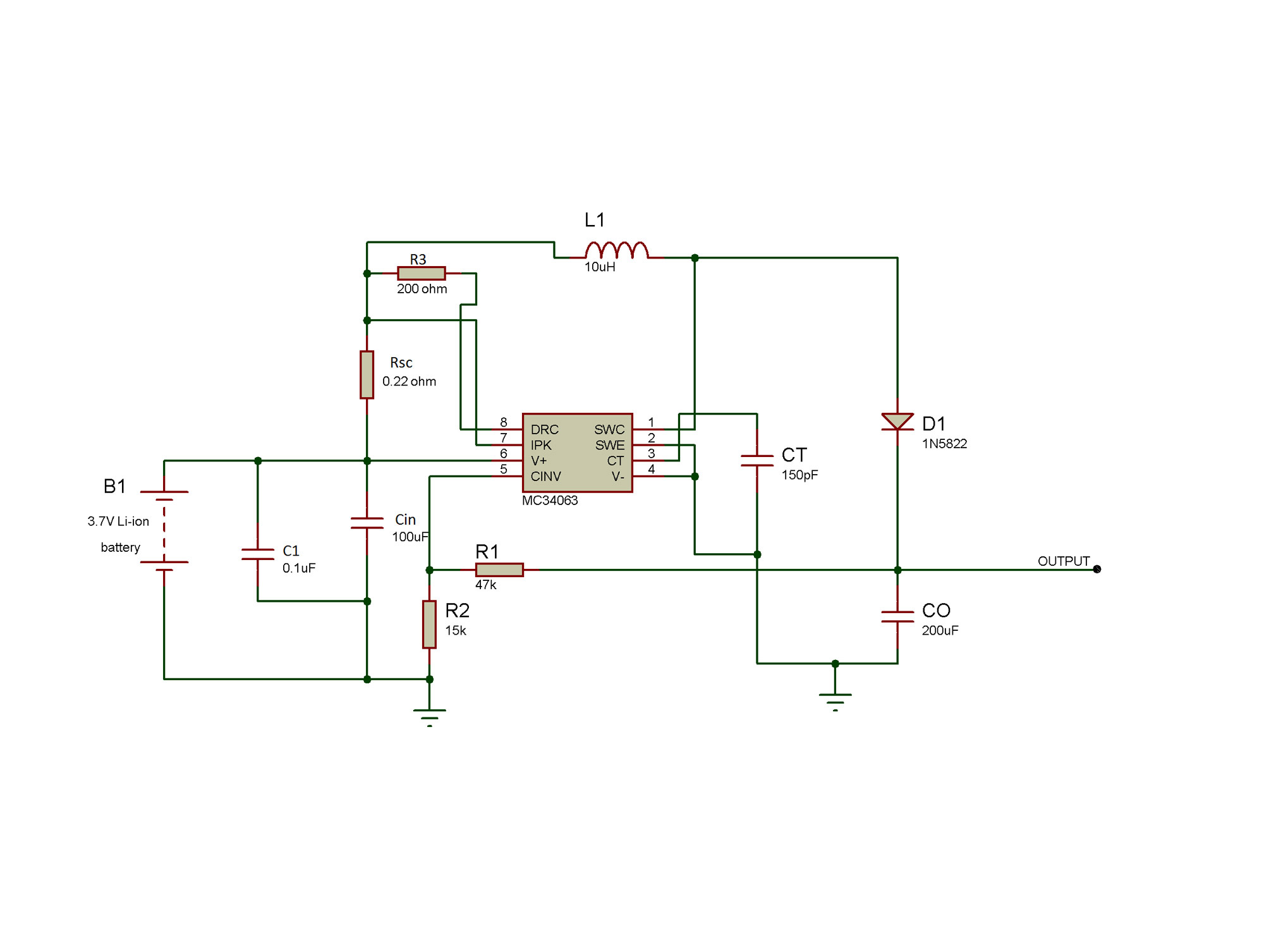
In this project, the boost converter circuit is built using the 34063A DC to DC converter IC. The input voltage is supplied through a 3.7 V battery which has its anode connected to the pin 6 of the regulator IC and cathode connected to the common ground. A capacitor Cin is connected at the pin 6 for removing ripples from the input signal. An additional capacitor C1 is connected parallel to capacitor Cin to reduce the overall ESR of the capacitances. The output voltage is drawn from the pin 5 of the regulator IC through a voltage divider circuit formed by resistances R1 and R2. At pin 7 of the IC, a current limiting resistor Rsc is connected and at pin 8, a resistance R3 is connected to limit the current at the base of inbuilt transistor of the IC. The pin 2 and 4 of the IC are grounded. At pin 1, an inductor and diode are connected to step up the input voltage. At pin 3 of the IC, a timing capacitor Ct is connected. There is a capacitor Co connected at the output of the circuit to reduce the ripples in the output signal.
How the circuit works –
Before understanding the operation of 34063 IC based boost converter circuit, it is important to understand how a basic boost converter circuit works. The following is the basic circuit of a boost converter.

Fig. 2: Circuit Diagram of basic Boost Converter
In a boost converter circuit, the output is greater than the input voltage signal. The basic circuit of a boost converter consists of an oscillator for providing the input signal, a diode, one switching component like the transistor and at least one charge storing element (capacitor or inductor).
The oscillator provides a square wave at the input so during the positive half-cycle of the square wave, the inductor stores some energy and generates a magnetic field. During this phase left terminal of the inductor is at a positive voltage. The base of the transistor gets positive voltage and it turns ON. Therefore, the anode of the diode is at lower potential and acts like an open circuit. So all current from the supply flows through the inductor to the transistor and finally to the ground.

Fig. 3: Circuit Diagram showing Positive Cycle in operation of Boost Converter Circuit
During the negative half cycle, the MOSFET turns off. Due to this the inductor does not get a path to charge up. The current through the inductor generates a back emf (as per the lenz law) which reverses the inductor polarity (as shown in below image). So the diode gets forward biased.
Now the inductor stored charge starts discharging through the diode and a voltage of higher level is obtained at the output. In this case, the output voltage depends upon the stored charge in the inductor. The more the stored charge is, the more the output voltage is obtained. Therefore if the charging time of inductor is more, then, the stored charge in the inductor also increases. So, there become two sources of input voltage – one is inductor and another one is input supply. So the output voltage is always greater than the input voltage.

Fig. 4: Circuit Diagram showing Negative Cycle in operation of Boost Converter Circuit
For increasing the efficiency and to remove the ripples from the output of the boost converter some other components need to be added in the basic circuit of the boost converter.
Designing a boost converter circuit using 34063 regulator –
In this project, a DC to DC converter is designed using the 34063 regulator IC. This regulator is a specially designed IC for DC-DC convertion. It provides a constant and regulated output voltage. Internally this regulator has a transistor with an oscillator where the oscillator provides up to 100 kHz square wave frequency.
The input signal for the operation of 34063 regulator can vary from 3V to 40 V and the output voltage can be adjusted as per the requirement using a voltage divider network. The IC can be used in boost converter, buck converter and voltage inverter applications. The IC has 8 pins with the following pin configuration –

Fig. 5: Table listing pin configuration of 34063 regulator IC
The regulator IC comes packed with the following features –
• Low Standby Current – Draw very less current when no load is connected to the output.
• Can provide output current up to 1.5 A by changing the external circuitry of this boost converter.
• Adjustable output voltage – user can change the output voltage as per the requirement.
• Adjustable Frequency up to 100 kHz

Fig. 6: Internal circuit of 34063 Regulator IC
From the figure 2 it can be seen that along with the basic components like oscillator, transistor, diode and inductor which are essentially part of the basic circuit design of a boost converter (figure 1), the 34063 regulator has additional components as well. These components are used to provide more features to the user and increase the efficiency of the boost converter circuit.
The following circuit is used to make a boost converter using the 34063 regulator –

Fig. 7: Circuit Diagram of Boost Converter
The different external components interfaced with the regulator IC serve the following specific functions –
Timing Capacitor CT- There is a capacitor connected at pin 3. The pin 3 has a function of timing capacitor. The capacitor connected at pin 3 sets the switching frequency for the regulator IC.
Current Limiting Resistor Rsc -There is a current limiting resistor connected at pin 7 of the regulator IC. The source current resistance Rsc is connected between the pin 7 and the positive terminal of the battery. The resistance Rsc limits the peak current Ipk (maximum internal current which flows from inductor and diode) from the circuit. That is why while designing the circuit, it is important to choose the right inductor and diode which can allow the maximum current Ipk.
Capacitances Cin, Co and C1 – There are capacitors Cin, Co and C1 connected in the circuit for filtering the input and output signals. The capacitances Cin and Co are used at the input and output respectively. These capacitors reduce the unwanted ripples and noise at the input and output signals. The Co capacitor provides a regulated and smooth DC voltage at the output. An additional capacitor C1 of very small value is also used in parallel with the capacitor Cin to reduce the ESR (Equivalent Series Resistance) at the input voltage.
Resistances R1, R2 and R3 – There are feedback resistors R1, R2 and R3 connected in the circuit. The R1 and R2 are the feedback resistors which decides the desired output voltage. The output voltage is dependent on the feedback resistors by the following equation –
Vout = Vref*(1+(R2/R1))
The voltage Vref is the reference voltage. Internally the 34063A provides a stable reference voltage of 1.25 V. For a desired output voltage the values of feedback resistors R1 and R2 can be calculated as follow –
Vout = 1.25*(1+(R2/R1))
5 = 1.25*(1+(R2/R1)) (Since desired output voltage, Vout = 5V)
By calculating above equation,
R2 = 3*R1
If R1 is taken to be 15k ohm
R2 = 3*15000
R2 = 45k ohm This can be round off to 47K ohm as 47k resistor is easily available.
So in this experiment
R1 = 15k and R2 = 47k
The resistor R3 is used to limit the current which flows to the collector of transistor which is inbuilt in the regulator(refer fig 2)
Inductor L1 and Diode D1 – The inductor and diode are the key components of basic boost converter circuit. The diode chosen to be used in the circuit is 1N5822 as this diode has less forward voltage drop, high current capability upto 3 A and can work in high frequency.
For designing a boost converter which converts the minimum input of 3.5 V to 5V output using 34063, the value for different external components has to be calculated as shown in Figure 3. According to the datasheet of 34063, for step up converter the following table can be used for calculating the component values. But before calculating the component values it is important to consider following parameter which are used in the table given in the datasheet.
(Minimum input voltage of the battery), Vin (min) = 3.5 V
(Required output voltage), Vout = 5V
(Maximum output current), Iout(max)= 500 mA
(Saturation voltage of the transistor), Vsat = 0.5 V (approx. value as per the datasheet of 34063)
(Forward voltage drop of the diode 1N5822), VF = 0.4(as per the datasheet of 1N5822 diode)
(Desired output switching frequency), f = 100 kHz
In the design of this boost converter circuit, maximum frequency which 34063AP1 regulator can provide is chosen. Due to the fact that higher the frequency smaller the size of the inductor, so this makes the circuit less bulky.
(desired peak−to−peak output ripple voltage), Vripple= 100 mV
This is the peak to peak ripple voltage which has to be considered at the output. The ripple voltage must be always less for a regulated and constant output.
Table for calculating the components values of Step−Up converter

Fig. 8: Table used for calculating the components values of Step−Up converter
For convenience the following values have been rounded off, so that components can be easily assembled.
CT = 150pF , Rsc = 0.22 ohm, Lmin = 10uH , Co = 200uF
Other components values
Resistance R3- The standard value of R3 resistor is 180 ohm for the step-up converter according to the datasheet of 34063 regulator. In the circuit it has been round off to 200 ohms.
Capacitor Cin – In this circuit, a capacitor of 100 uF is used for Cin. This is the standard value for the step-up converter according to the datasheet of the 34063 regulator.
Capacitor C1 – The value of C1 capacitor must be less so that it can reduce the overall ESR, so the capacitance C1 is taken 0.1uF
After connecting all the external components with the regulator IC, output voltage and current can be measured for practical observations. The measurement of different voltage and current values in the circuit helps in judging the efficiency of the boost converter circuit.
Practical input voltage of the battery, Vin = 3.6 V
Practical output voltage, Vout = 5.35 V
The efficiency of the boost converter circuit need to be judged with different loads. For convenience resistors of different values are connected as load at the output for testing. The results obtained during the test are summarized in the following table –

Fig. 9: Table listing output voltage and current from Boost Converter for different loads

Fig. 10: Graph showing Voltage variation for different loads at boost converter output

Fig. 11: Graph showing Current variation for different loads at boost converter output
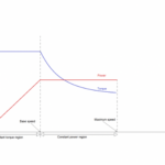
From the practical observations, it can be seen that when the current demand increases then the voltage starts dropping out. Like for 5V output voltage with a load of 100 ohms, the current drawn at the output is 50 mA. As the voltage output starts falling below 5V, the current drawn by the load starts increasing. Hence, the circuit can only provide up to 50 mA current approximately if the output voltage is set to 5V approximately. The efficiency of the circuit can be improved by adding filters and Voltage Regulators (Zener Diodes) to get a Regulated voltage at output.

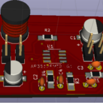
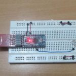
Fig. 12: Prototype of Boost Converter designed on a Breadboard
In designing this circuit it is important that for stabilized output, use of capacitor at the input supply and also at the output of the circuit is must, so that the unwanted ripples from the input and output signals can be reduced. A low value of the capacitor (C1) should also be added in parallel with a high value of the capacitor (Cin) at the input to reduce the overall ESR. The diode and inductor must be chosen wisely so that they can allow maximum input current (Ipk) through them. Maximizing the current at the output should be the criteria for choosing the diode and the inductor. The input supply must be provided to the 34063 regulator in its working range only. The selection of the diode (D1) should be such that it takes less forward voltage drop across it and can work on high frequencies.
You may also like:

Circuit Diagrams
Filed Under: Electronic Projects

Questions related to this article?
👉Ask and discuss on EDAboard.com and Electro-Tech-Online.com forums.
Tell Us What You Think!!
You must be logged in to post a comment.