In the previous tutorial, different types of SMPS have been already discussed. In this series, following SMPS circuits will be designed –
1. Boost Converters –
a) Open Loop Boost Converter
b) Closed Loop Boost Converter
c) Open Loop Boost Converter with Adjustable Output
d) Closed Loop Boost Converter with Adjustable Output
2. Buck Converters –
a) Open Loop Buck Converter
b) Closed Loop Buck Converter
c) Open Loop Buck Converter with Adjustable Output
d) Closed Loop Buck Converter with Adjustable Output
3. Buck-Boost Converters
a) Open Loop Inverting Buck – Boost Converter
b) Open Loop Inverting Buck – Boost Converter with Adjustable Output
4. Flyback Converter
5. Push-Pull Converter
In this tutorial, an open loop boost converter SMPS will be designed. The Boost Converter is one of the topologies of Switched Mode Power Supply (SMPS). It has a DC source as Input power like a battery, generator or rectifier. In case of a boost converter, the output power is always greater than the input power. So, the boost converter circuit will step up the power from one DC level to a higher DC level. The method of converting one DC voltage to a different DC voltage is called DC to DC conversion. The boost converter is a DC to DC converter which steps up the input signal to the higher voltage level.
The boost converter can be designed in two ways-
Open loop boost converter – In open loop boost converter, there is no feedback from output to input contrary to the closed loop which has a feedback circuit. So, the output of an open loop boost converter is not regulated.
Closed loop boost converter – In closed loop boost converter, there is a feedback from the output to the input. So, the output of a closed loop boost converter is regulated.
There are certain design parameters involved in the designing of the boost converter. It is important to understand these design parameters. Any boost canverter can operate in either of the twopossible modes of operation. These modes of operation are as follow –
• Continuous Conduction Mode (CCM)- In CCM, the current in the inductor is continuous in the entire cycle of the switching period. So a regulated voltage at the output is obtained but the output is regulated only if the current is drawn within the limits of CCM.
• Discontinuous Conduction Mode (DCM)- In this mode, the current in the inductor is pulsating and it becomes zero for a part of switching time. So a regulated voltage is not received in DCM. But, the voltage can be regulated by connecting a feedback circuit from output to input.
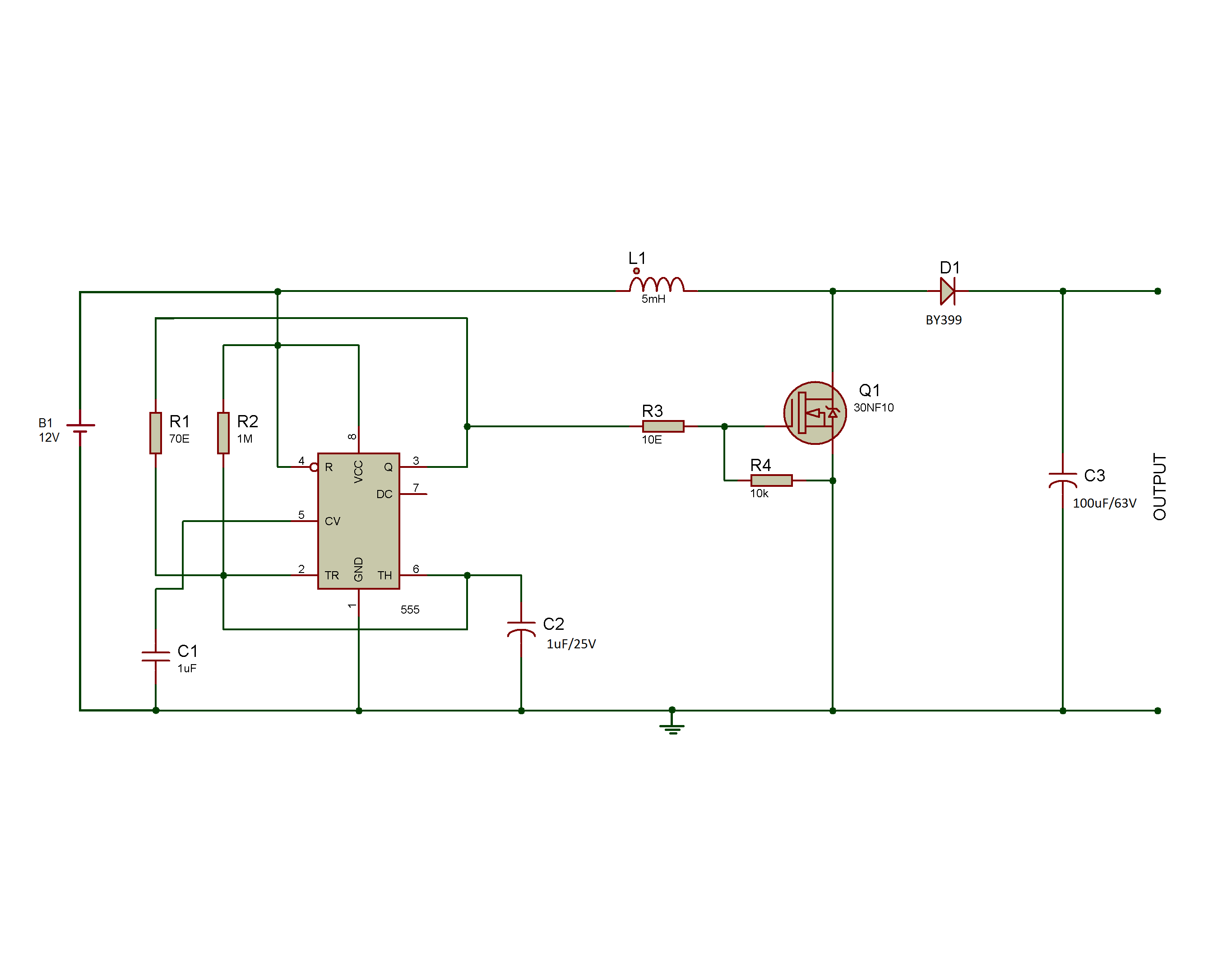
In this tutorial, a non-isolated boost converter is designed which means the input and output share the same ground. The boost converter designed in this project will step up 12V DC to 24V DC with a tolerance limit of +/-0.5V. Once the circuit is designed and assembled, the value of the output voltage and current will be observed using a multimeter. These values will indicate the efficiency of the boost converter designed in the project.
Components Required –

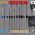
Fig. 1: List of Components required for Open loop Boost Converter SMPS
Block Diagram –

Fig. 2: Block Diagram of Open loop Boost Converter SMPS
Circuit Connections –
In this experiment, an open loop boost converter operating in CCM mode is designed and the component values as per the CCM standard equations are calculated for the desired output.
The boost converter has the following circuit blocks –
1. DC source – A 12V Battery is used as the input power source in the circuit.
2. 2. Oscillator and switching mechanism – An Oscillator is used to generate a Pulse Width Modulated (PWM) signal of a desired frequency. In this boost converter, 555 IC is used to generate the PWM signal so, 555 IC is acting like an oscillator. The PWM signal is a train of the pulse which is used to turn ON and OFF the MOSFET. The MOSFET is used as the switching transistor in the circuit. The 555 is configured in its Astable mode with some modification in the basic circuit. In order to learn that how 555 IC generates PWM signal, read ‘Generating Square Wave’ tutorial.
It should be taken care that the input voltage of 555 should not exceed beyond the specified limit mentioned in its datasheet. A pulled down capacitor should always be used at the control pin of the 555 IC for avoiding unwanted noise from the surroundings.
For switching purpose, a transistor and a diode are used as a switching component. For the selection of the transistor, MOSFET is chosen as FETs are known for their fast switching speed and low RDS (ON) (drain to source resistance in ON state). So an N-channel 30NF10 MOSFET (shown as Q1 in the circuit diagram) is connected parallel to the input DC source which acts like a switch in the circuit. The switching time of the MOSFET and diode should be less than the rise and fall time of the PWM wave. The diode should offer low voltage drop in forwarding bias and the RDS (ON)of the MOSFET should be low.
A gate to source resistance must be used to avoid any unwanted triggering of the MOSFET by external noise. It also helps in fast turning OFF the MOSFET by discharging its parasitic capacitance. A low value of the resistor (10E to 500E) should be connected to the gate of the MOSFET. This will solve the problem of ringing (parasitic oscillations) and in rush current in the MOSFET. The voltage level of the PWM signal should be greater than the threshold voltage of the MOSFET. So that the MOSFET can be turned ON fully with minimum RDS (ON ).
Another switching component used in the circuit is a diode. The switching time of the diode should be less than the rise and fall time of the PWM wave. The 555 IC that has been used generates a PWM wave having rise time 110ns and fall time of 90ns. The forward voltage drop of the diode should also be very low otherwise it will dissipate power which will further reduce the efficiency of the circuit. So in this experiment, a BY399 diode is selected which suits best to the circuit design.
Before generating the PWM signal the switching frequency for the circuit needs to be decided. For this boost converter, a switching frequency of 10kHz is selected which will work fine this converter design.
The duty cycle of the generated PWM signal is another important consideration as it will decide the active state of the MOSFET. The duty cycle can be calculated as follows –
D% = 1- (Vin/Vo)*100
Vo=Desired output voltage, 24V
Vin =Input voltage, 12V
By putting all the values in the above equation, the desired duty cycle is –
D = 50%
A capacitor and resistor of the appropriate value should be used for generating the 10kHz frequency and 50% duty cycle. The higher is the frequency selected for switching components, the higher are the switching losses. This decreases the efficiency of the SMPS. But high switching frequency reduces the size of the energy storage element and improves the transient response of the output.
3. Energy Storage Element
An inductor is used for storing the electrical energy in the form of magnetic field. So the inductor acts like an Energy Storage Element. The value of the inductor can be calculated using the standard equation of CCM which is as follows –
Lmin>= Vo /(16* Fs*Io (min))
where, Lmin = Minimum value of inductor
Fs = 10kHz
Io (min) = Critical value of output current to maintain a regulated voltage at the output.
Assuming Io (min) = 30mA
By putting all the values in the above equation, the value of inductor is obtained as follow –
Lmin>= 5mH
The value of the inductor should be as per the calculation and its current rating should be greater than the peak current of inductor (Standard equation of CCM, Peak current, Ipk = (Vin*D*Ts)/L)
4. Output Filtering Element
As a filtering element, a capacitor (shown as C3 in the circuit diagram) is used at the output of the circuit. In normal operation of Boost circuit, the transistor Q1 turns ON and OFF according to the frequency of the oscillator circuit. This generates a train of the pulse at the inductor L1 and capacitor C3 as well as transistor Q1. As the capacitor is connected with inductor only in the negative cycle of the PWM signal, this makes an LC filter which filters the train of the pulse to produce a smooth DC at the output. The value of the capacitor can be calculated by using following equation of CCM – Cmin>= (Io (max) * D)/ (Fs*dVo)
Where, Cmin = Minimum value of capacitor
Maximum current at the output, Io (max) = 100mA
Duty cycle, D = 0.5
Desired output ripple voltage, dVo
Assuming dVo= 100mV
By putting all the values in the above equation the capacitance value is obtaained as follow –
Cmin>= (0.01 * 0.5)/ 10000*0.01
Cmin>= 50uF
C >= (0.01 * 0.5)/ 10000*0.01
C >= 50uF
As it is the minimum value of capacitor required, so in the circuit a capacitor of standard value is used which can be easily available, so, capacitor of 100 uF is taken.
C3= 100uF
The capacitors used in the circuit must be of higher voltage rating than the input supply voltage. Otherwise, the capacitors will start leaking the current due to the excess voltage at its plates and will burst out. All the capacitors should be discharged before working on a DC power supply application. For this, the capacitors can be shorted with a screwdriver wearing insulated gloves.
How the Circuit Works –
Any SMPS has some switching components which turn on and off at high frequency and has some storage component which stores the electrical energy while the switching components are in the conduction state and discharge the stored energy to the output device while the switching components are in the non-conduction state.
A simple Boost Converter consists of the inductor(L), a diode(D), a capacitor(C) and a transistor where transistor acts like a switch. In the boost circuit, when the switch is closed i.e. the switching component is in a conduction state, the inductor starts generating a magnetic field and stores energy. The stored energy in the inductor steps up the output voltage in comparison to the input voltage.
When current starts flowing through the switching component as its path is less resistive compared to the path in parallel which contains capacitor and the output load, the inductor generates a positive polarity at its left terminal and negative to the right terminal. Due to change in polarity, the diode gets reverse biased. In this condition, the capacitor, which was charged in the previous cycle, provides the current to the load while the switching component goes in non-conduction state or goes open between the ground.

Fig. 3: Circuit Diagram showing ON state of switching Component in Boost Converter
When the switch is open the current is reduced as the impedance increases so the generated magnetic field in the inductor starts collapsing and the polarity of the inductor reverses. This makes the diode forward biased and the capacitor now starts charging with a voltage greater than the input voltage. As the input is now having two sources in series one is the inductor and another is the battery. So the output voltage is always greater than the input voltage.

Fig. 4: Circuit Diagram showing OFF state of switching Component in Boost Converter
So, in ON state, the Diode was in blocking Mode (OFF) and the Transistor was ON. In OFF state, the Diode was in conducting mode (ON) and the Transistor was OFF.
So, it can be said that the Boost Converter is having two switching components – one is the transistor and another one is the diode. At a time only one of the switching component conducts i.e. it is in ON state while the other goes in non-conduction state i.e. it goes in OFF state.
Testing the circuit –
First of all, the PWM output from the 555 circuit should be confirmed. The output waveform by the oscillator circuit or 555-timer can be observed on an oscilloscope. The waveform generating on the circuit is obtained as shown in the figure below –

Fig. 5: Graph showing PWM output from 555 IC based circuit as obseeved on a CRO
On measuring voltage and current values with different loads at the output, following observations were taken –
Battery Voltage, Vin = 12V
Vout

Fig. 6: Table listing output voltage and current from Open Loop Boost Converter SMPS for different loads
So, it can be observed that in the tolerance limit of +/-0.5V the output current of 49.5mA is obtainable.

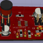
Fig. 7: Prototype of Open Loop Boost Converter SMPS designed on a Breadboard
But since the maximum output current should be 100mA for 24V, there is a drop in voltage due to the losses in the circuit like switching and conduction losses of diode and MOSFET, losses in the windings that surround the core of inductor , eddy current losses and hysteresis losses in the inductor, capacitor losses due to ESR (Equivalent Series Resistance) and losses due to Rds(on) of N-MOS. The efficiency of the circuit is maximum when output current is 49.5mA. The efficiency of the circuit can be calculated as follow –
Efficiency % = (Pout/Pin)*100
(Output Power) Pout = Vout*Iout
(Output Voltage)Vout = 24.8V
(Output current) Iout = 49.5mA
Pout = 1228mW(approx.)
(Input Power) Pin = Vin*Iin
(Input Voltage) Vin = 12V
(Input Current) Iin = 115mA (measured the input current using ammeter)
Pin = 1380mW
By putting all the values,
Efficiency % = 88%
It can be seen that there are certain limitations of this circuit. The output voltage in this circuit is not regulated it varies for different load resistances. This can be improved by adding a feedback circuitry which helps in regulating the output voltage. A Boost Converter with feedback circuit is designed in the next tutorial. Secondly, the efficiency of this boost converter design is 88% due to the power losses in the circuit.
This is an open loop boost converter with non-isolated output and operating in CCM mode. It can be used as switching regulator for LED drivers and as a regulated DC power supply. It can be used for supplying power to low power portable electronic devices. In battery powered applications when there is a space restriction to stack the number of batteries in series for achieving high voltage, this boost converter can be used with less number of batteries to supply the DC power.
This boost converter is simple to design and use cheap components. It can be easily assembled in no time. Also, there is no need of control circuitry for PWM signal generation in this boost converter design.
You may also like:

Circuit Diagrams
Project Video
Filed Under: Tutorials
Filed Under: Tutorials

Questions related to this article?
👉Ask and discuss on Electro-Tech-Online.com and EDAboard.com forums.
Tell Us What You Think!!
You must be logged in to post a comment.