There are 2 cut off frequencies for band reject filter.
1. upper cut off frequency (f1) – the frequency below which all the frequencies are passed
2. lower cut off frequency (f2) – all the frequencies above this frequency are passed
Similar to band pass filter but the difference is f1 < f2. That means upper cut off frequency is lesser than lower cut off frequency. Two types of band reject filters are
1. Wide band reject filter – suppresses wide range of frequencies.

Fig. 1: Overview of Wide Band Reject Filter
2. Narrow band pass filter – suppresses single frequency or few frequencies near centre frequency.
Wide Band Reject filter
It’s actually combination of LPF and HPF as shown in figure
Here F1 > F2. So we have to design HPF with F1 and LPF with F2. Suppose we want to suppress the band of frequencies between 10 KHz to 20 KHz. so F1 = 20000 Hz and F1 = 10000 Hz.
Designing HPF section
Step 1: assume the required value of capacitor. it should be less than 0.1 micro Farad. This is required for better frequency stability. Suppose we assume value C as 1 nF (nano farad)

Fig. 2: Screenshot of calculations required to find resistance and pass band gain for HPF Section
Designing LPF section
Step 4: assume the required value of capacitor. Suppose we assume value C as 10 nF

Fig. 3: Screenshot of calculations required to find resistance and pass band gain for LPF Section
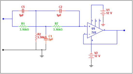
Final design with component values are as shown. Op-amp is active component and it requires +ve and -ve biasing voltages. one can test the circuit by applying input through signal generator and observing output on DSO or oscilloscope as well as bode plotter as shown in figure.

Fig. 4: Circuit Diagram of LM741 OPAMP IC based Band Reject Filter
Note: – the schematic design is prepared in NI’s multisim 11 software. Software is available as free for 1 month trial period from NI’s website.
Narrow Bank Reject Filter (Notch Filter)
Step 1: select notch frequency that is the frequency to be rejected. Mostly such filters are used to remove power line frequency that is 50 Hz. So take Fn = 50 Hz
Step 2: assume capacitor value C as 1 micro F (because frequency is too low the capacitor value should be large)

Fig. 5: Screenshot of calculations required to find resistance for Notch Filter
Step 5: to construct T network with C – R/2 – C, we need R/2 value. So connect two resistors in parallel of same value R
Step 6: to construct T network with R – 2C – R, we need 2C value. So connect two capacitors in parallel of same value C
Final design is as shown below.

Fig. 6: Circuit Diagram of LM741 OPAMP IC based Notch Filter
You may also like:


Circuit Diagrams
Project Video
Filed Under: Circuit Design, Electronic Projects
Filed Under: Circuit Design, Electronic Projects

Questions related to this article?
👉Ask and discuss on EDAboard.com and Electro-Tech-Online.com forums.
Tell Us What You Think!!
You must be logged in to post a comment.