The Push-Pull Converter is one of the topology of SMPS. In this series, following SMPS circuits are designed –
1. Boost Converters –
a) Open Loop Boost Converter
b) Closed Loop Boost Converter
c) Open Loop Boost Converter with Adjustable Output
d) Closed Loop Boost Converter with Adjustable Output
2. Buck Converters –
a) Open Loop Buck Converter
b) Closed Loop Buck Converter
c) Open Loop Buck Converter with Adjustable Output
d) Closed Loop Buck Converter with Adjustable Output
3. Buck-Boost Converters
a) Open Loop Inverting Buck – Boost Converter
b) Open Loop Inverting Buck – Boost Converter with Adjustable Output
4. Flyback Converter
5. Push-Pull Converter
The Push-Pull is a DC to DC converter which uses a transformer for changing the DC power. The output voltage of push-pull converter is either less than or greater than the input supply voltage. It is one of the topologies of the Switched Mode Power Supply so it works on the principle of switching regulators. In Push-Pull converter, the current is drawn in both halves of the switching cycle contrary to other converters like Buck-Boost or Flyback converter. This gives a more steady current at the output.
Contrary to Linear Regulators, Push-Pull Converters use switching regulators. That is why, the voltage is not altered by heat dissipation and the law of power conservation applies to these converter circuits. According to the law of power conservation, input power must be equal to output power.
Pin = Pout
Vin*Iin = Vout*Iout
In Boost Mode of Push-Pull Converter, Input voltage is less than output voltage, so the output current is less than the input current. While in Buck Mode of Push-Pull Converter, Input voltage is greater than output voltage, so the output current is greater than the input current. Therefore, SMPS can also Buck or Boost the output current along with voltage which increases its efficiency as compared to linear regulators.
The Push-Pull Converter can be designed in two ways –
Open loop Push-Pull Converter – In open loop Push-Pull converter, there is no feedback from output to input contrary to the closed loop which has a feedback circuit. So, the output of an open loop Push-Pull converter is not regulated.
Closed loop Push-Pull Converter – In closed loop Push-Pull converter, there is a feedback from the output to the input. So, the output of a closed loop Push-Pull converter is regulated.
There are certain design parameters involved in the designing of the Push-Pull converter. It is important to understand these design parameters. Any Push-Pull converter can operate in either of the two possible modes of operation. These modes of operation are as follow –
Continuous Conduction Mode (CCM)- In CCM, the current in the inductor is continuous in the entire cycle of the switching period. So a regulated voltage at the output is obtained but the output is regulated only if the current is drawn within the limits of CCM.
Discontinuous Conduction Mode (DCM)- In this mode, the current in the inductor is pulsating and it becomes zero for a part of switching time. So a regulated voltage is not received in DCM. But, the voltage can be regulated by connecting a feedback circuit from output to input.
In this tutorial, an isolated Push-Pull converter is designed which means the input and output have different ground. The Push-Pull converter designed in this project will have adjustable output between 12V DC and 24V DC. Once the circuit is designed and assembled, the value of the output voltage and current will be observed using a multimeter. These values will indicate the efficiency of the Push-Pull converter designed in the project.
Components Required –

Fig. 1: List of Components required for Open Loop Isolated Push-Pull Converter
Block Diagram –

Fig. 2: Block Diagram of Open Loop Isolated Push-Pull Converter
Circuit Connections –
In this project, an open loop Push-Pull converter is designed. The Push-Pull converter has the following circuit blocks –
1. DC source –
A 12V Battery is used as the input power source in the circuit.
2. Oscillator and Switching Mechanism –
For switching purpose a transistor and a diode are used as switching components.
The switching components has to operate on a specific frequency. This frequency is generated through an oscillator circuit. In this project, Arduino UNO is used to generate a PWM signal which provides the required frequency. Any other Arduino Board like Arduino Mega can also be used. In fact any microcontroller or microcontroller board which can output PWM can be used in the circuit. Arduino is chosen as it is the most popular prototyping board and can be easily programmed. Due to large community support, it is easy to learn and work on Arduino. The PWM signal is a train of the pulse which is used to turn ON and OFF the MOSFET. The MOSFET is used as the switching transistor in the circuit.
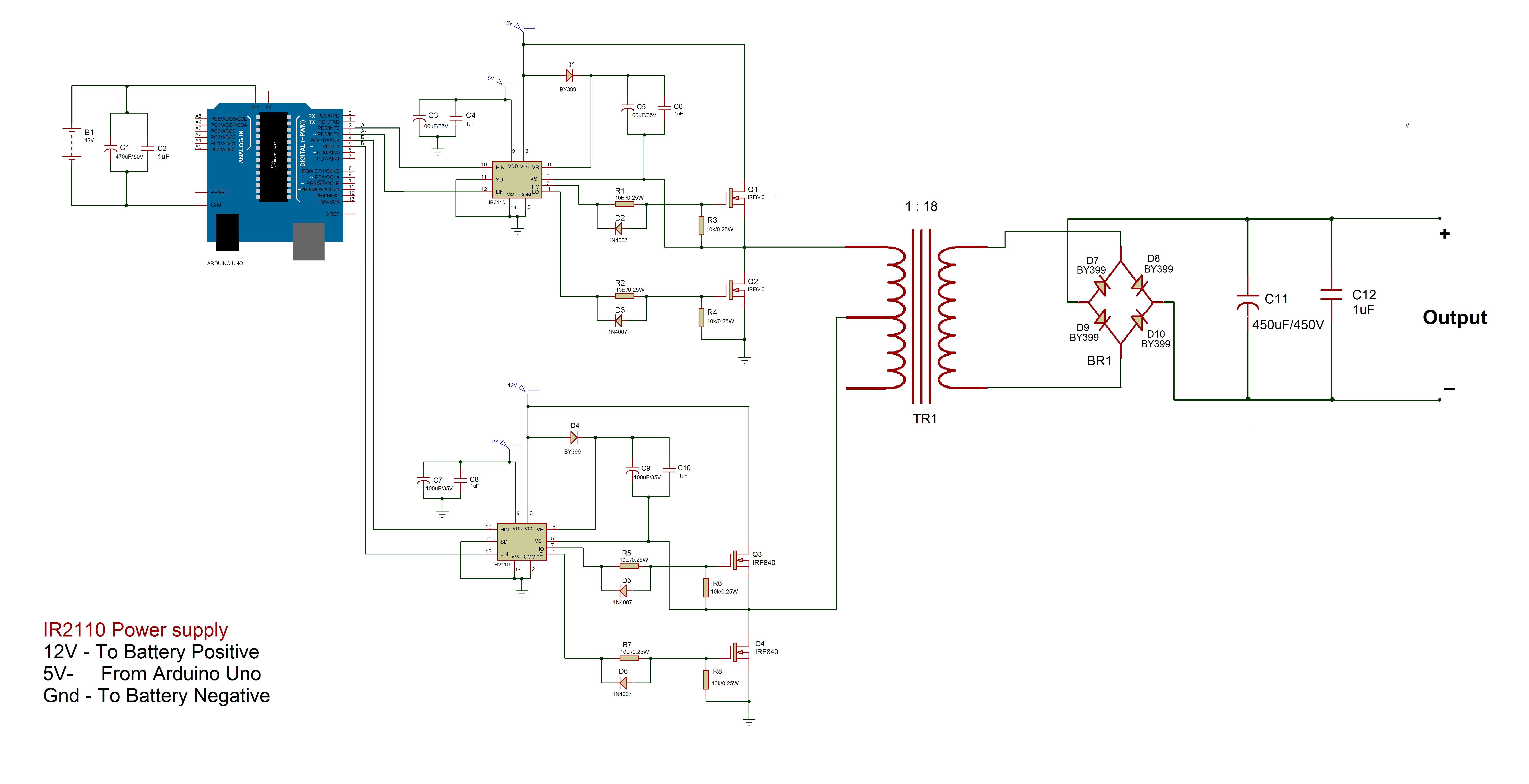
For switching purpose, a transistor and a diode are used as switching components. For the selection of the transistor, MOSFET is chosen as FETs are known for their fast switching speed and low RDS (ON) (drain to source resistance in ON state). In this configuration, the MOSFET is connected in high-side configuration. As in high side, the N-channel MOSFET requires a Bootstrap Circuitry or a Gate Driver IC for its triggering, this makes the driver more complicated. In this configuration, four N-MOSFET are used of which two are in high-side configuration (shown as Q1 and Q3 in the circuit diagram) and other two are in low-side (shown as Q2 and Q4 in the circuit diagram) making a full bridge circuit. The MOSFET used in the circuit has its threshold voltage around 10V to 12V.
The switching time of the MOSFET and diode should be less than the rise and fall time of the PWM wave. The diode should offer low voltage drop in forward bias and the RDS (ON)of the MOSFET should be low. Always a gate to source resistance should be used to avoid any unwanted triggering of the MOSFET by external noise. It also helps in fast turning OFF the MOSFET by discharging its parasitic capacitance. A low value of the resistor (10E to 500E) can be used at the gate of MOSFET. This will solve the problem of ringing (parasitic oscillations) and inrush current in the MOSFET. The voltage level of the PWM signal should be greater than the threshold voltage of the MOSFET. So that the MOSFET can be turned ON fully with minimum RDS (ON ) .
It is important that the connection of all the four MOSFET should be properly checked before attaching the battery. The input power supply of the controller, IC, and MOSFET should also be checked beforehand and it should be ensured that the power supply is in the range of all the components. It should be ensured that the input signal to the driver from the controller is correct. The high side and low side input waveform should not overlap as it turns ON both the low and high side MOSFET which can cause a short circuit. An oscilloscope can be used to ensure that no signals are overlapping.
The MOSFET cannot be triggered by the microcontroller as the microcontroller can generate a 5V PWM signal only. Therefore an additional IC IR2110 is used in the circuit to generate a PWM signal of 12V and the input to the IR2110 is provided by the microcontroller. IR2110 is a high and low side driver. It is a high speed (operational at high frequency) power MOSFET and IGBT driver with independent high and low side referenced output channels. The floating channels can operate up to 500V or 600 V. The IC is 3.3V logic compatible that is why it can be used with any microcontroller. The IC comes in a 14 Lead PDIP package. IR2110 has the following pin configuration –

Fig. 3: Table listing pin configuration of IR2110 IC
It should be ensured that the ground of controller and the driver IC is same and the driver input and output ground should also be common.
Another switching component used in the circuit is a diode. The switching time of the diode should be less than the rise and fall time of the PWM wave. The Arduino board generates a PWM wave having rise time 110ns and fall time of 90ns. The forward voltage drop of the diode should also be very low otherwise it will dissipate power which will further reduce the efficiency of the circuit. The diode should offer low voltage drop in forward bias and the RDS (ON)of the MOSFET should be low. So in this experiment, a BY399 diode is selected which suits best to the circuit design.
Before generating the PWM signal the switching frequency for the circuit needs to be decided. For this push-pull converter, a switching frequency of 1kHz is selected as the transformer used in the circuit will start saturating beyond this frequency.
The duty cycle of the generated PWM signal is another important consideration as it will decide the active state of the MOSFET. The duty cycle can be calculated as follows –
Vout = Vpeak*D
Desired output voltage, Vout= 24V
D = duty cycle
Vpeak = Voltage level of transformer output wave (secondary side)
The transformer used has 1:18 number of turns. So for the 12V input, it will give 220V at the output. Therefore,
Vpeak = 220V for 12V input
By putting all the values,
D = 24/220
D = 0.11
D% = 11%
For generating 1 kHz PWM signal having duty cycle of 11%, the Arduino board is programmed. The Arduino sketch required for generating the desired PWM output is attached in the tutorial. It can be downloaded and burnt to an Arduino board for use.
The higher is the frequency selected for switching components, the higher are the switching losses. This decreases the efficiency of the SMPS. But high switching frequency reduces the size of the energy storage element and improves the transient response of the output.
3. Transformer and Full wave rectifier –
In this circuit, a transformer having turns ratio 1:18 is used as energy storage element. The output of the transformer is connected to a full wave rectifier. The full wave rectifier converts the 220V AC to 220V DC. As full wave rectifier is more efficient than a half wave rectifier, it allows complete use of both the negative and positive side of signal. In full wave bridge rectifier configuration, four diodes are connected in such a way that it generates a DC signal at the output. During full wave rectification, at a time two diodes become forward biased and another two diodes are reversed biased.
For selecting diode for the full-wave rectifier, it is important to consider certain selection parameters. The switching time of the diodes should be less than the switching period of the rise and fall time of the PWM wave. The Arduino generates a PWM wave of the rise time of 110ns and fall time of 90ns. The forward voltage drop of the diode should also be very low otherwise it will dissipate power which will further reduce the efficiency of the circuit. That is why, BY399 diodes are used for making the full-wave rectifier as they can sustain reverse voltage up to 220V.
The transformer’s output impedance should be low so that less voltage drop occur at the output while connecting load. Such transformer should be chosen which can sustain the desired switching frequency. Otherwise the transformer will start saturating beyond its rated frequency and cause power losses in the circuit.
4. Output Filtering Element –
A capacitor C1 of high value is connected to the output of rectifier circuit. As the DC which is to be rectified by the rectifier circuit has many AC spikes and unwanted ripples, so to reduce these spikes using a capacitor is must. This capacitor acts as a filtering capacitor which bypasses all the AC through it to the ground. At the output, the DC left is then smoother and ripple free. A small value of ceramic capacitor C2 is also used in parallel with the capacitor C1 to reduce the overall ESR.
How the circuit works –
Any SMPS has some switching components which turn on and off at high frequency and has some storage component which store the electrical energy while the switching components are in conduction state and discharge the stored energy to the output device while the switching components are in non-conduction state.
In Push-Pull converter there are two pairs of the transistor which are shown as four switches in the circuit diagram below. These pair of transistors are like a Full bridge circuit and provides the input supply to the transformer. The input of the transformer is connected with the transistor pair and at an output, a full wave rectifier (BR1) and capacitor (C1) is used to convert the pulsating DC into pure DC. In OFF state when all the switches are open then the voltage at the output is zero.

Fig. 4: Circuit Diagram of Basic Push-Pull Converter
When switches SW1 and SW4 are closed, the switch SW1 pushes the transformer’s one end and the switch SW4 pulls down another end. That’s why this is called Push-Pull converter. This generates a voltage at the output of the transformer. The voltage is then rectified and smoothed by the output capacitor.

Fig. 5: Circuit Diagram showing Positive Cycle in Basic Push-Pull Converter
When switches SW2 and SW3 are closed, the current at the primary of the transformer reverses and at the output of the transformer, voltage opposite in polarity as earlier is obtained. Then again the pure DC is sent to the load by the rectifier and the output capacitor.

Fig. 6: Circuit Diagram showing Negative Cycle in Basic Push-Pull Converter
The transistor pairs switches ON and OFF periodically reversing the current in the transformer. Therefore current can be drawn from the line all the time. It is recommended to give a small delay while powering the transformer in one way and powering it to another way. As any pair of transistor if switch ON simultaneously then may cause the risk of short circuit. This delay is called dead time and is required to avoid the problem of shoot-through of the transistor.
The Push-Pull Converter is different from a square wave invertors. Inverters are meant for 50Hz frequency and 50% duty cycle while in Push-Pull converter the duty cycle, as well as the frequency for stepping up or stepping down the output voltage, can be varied. So in the Push-Pull Converter, the output voltage is dependent on the turn’s ratio of transformer and the duty cycle.
Testing the Circuit –
This Push-Pull Converter has an output between 12V DC and 24V DC.

Fig. 7: Prototype of Open Loop Push-Pull Converter designed on a breadboard
In this circuit, Input Voltage, Vin = 12V
On measuring voltage and current values with different loads at the output, following observations were taken –

Fig. 8: Table listing voltage and current outputs from Open Loop Isolated Push-Pull Converter for different loads
It can be observed that at the output, a voltage of 22V is obtained for maximum output current of 11mA. Also a high voltage at the output is received when no load is connected though it should be equal to the desired output voltage. This is due to the output capacitor. The capacitor keeps on charging until it becomes fully charged. So the voltage at the output is very high in the absence of load.
The power efficiency of the circuit can be calculated as follow –
Efficiency % = (Pout/Pin)*100
Input Power, Pin = Vin*Iin
(Input Voltage),Vin = 12V
The Input Current (Iin), is measured for all the three loads. So, Average Input Power for above three observations can be calculated as follows –
Pin = ((Vin1*Iin1)+(Vin2*Iin2)+(Vin3*Iin3))/3
Pin = ((12*0.16)+(12*0.18)+(V3*0.2))/3
Pin = 4W (approx.)
(Output Power) Pout = Vout*Iout
(Output Voltage), Vout
(Output current),Iout
Average Output Power for above three observations can be calculated as follows –
Pout = ((Vout1*Iout1)+(Vout2*Iout2)+(Vout3*Iout3))/3
Pout = ((68*6.8)+(43*8.5)+(22*11))/3
Pout = 357mW
Efficiency % = ((0.357)/4)*100
Efficiency % = 10% (approx.)
It can be seen that the output voltage in the circuit is not regulated and it varies for different loads. This can be improved by adding a feedback circuitry which helps in regulating the output voltage. The efficiency of the SMPS design is less as power losses in the circuit. are not considered. There are switching and conduction losses of diode and MOSFET, losses in the windings that surround the core of the transformer, eddy current losses and hysteresis losses in the transformer coil, capacitor losses due to ESR (equivalent series resistance), losses due to Rds (on) of N-MOS and the core losses in the transformer.
Project Source Code
###

//Program to
////// Code for Closed Loop Boost converter with variable output voltage ////////
////// Output Voltage Adjustment from 5V to 9V ////////

#define TOP 1599                  // Fosc = Fclk/(N*(1+TOP)); Fclk = 16MHz, Fosc = 10kHz
#define CMP_VALUE_HALF_DUTY 799    // 50% duty cycle
#define FeedbackPin A4             // Input pin of potentiometer at A4
#define Inputpin A5                // feedback pin of potentiometer at A5
#define R1plusR2_resistor 6.0    // variable of R1+R2 value
#define R1_resistor 1.0             // variable of R1 value
#define PWM 9                     // PWM(Pulse Width Modulation) wave at pin 9

//// function declaration
float Map_feedback(float);            //function to map feedback values
float Mapping_output_voltage(float); //function to map potentiometer values
void InitADC(void) ;                 // Function to start ADC conversion
uint16_t ReadADC(uint8_t);            // function to read Analog value

 ///// function definition   ////////
float Mapping_output_voltage(float Input_Read ){

float Compare_voltage = (((Input_Read*(1.0)/1024)*4)+5);   // mapping the digital value
return(Compare_voltage);                               // return the calculated output voltage
}

void InitADC(void){

ADMUX &= ~((1<<REFS1)|(1<<REFS0));           // for setting Aref = AVcc , internal Aref turns OFF
ADCSRA = (1<<ADEN)|(1<<ADPS2)|(1<<ADPS1)|(1<<ADPS0);    //Prescalar div factor =128
}

uint16_t ReadADC(uint8_t channel_number)  {

//clear other than last three bits of the channel_number
channel_number &= 0x07;
//clear last 3 bits of ADMUX, OR with channel_number
ADMUX =  (ADMUX & 0xf8) | channel_number;
//start ADC conversion
ADCSRA|=(1 << ADSC);
//wait for conversion to complete
while((ADCSRA) & (1<<ADSC));
//return ADC value
return(ADC);
}

float Map_feedback(float Digital_Read){

float ADC_READ = (Digital_Read/1024.0)*3.33;            // converting digital values
float output_voltage  = (ADC_READ*(R1plusR2_resistor/R1_resistor));  // calculating output voltage
return(output_voltage);                                // return the calculated output voltage
}
////////// function definition complete//////////

void setup() {
  // put your setup code here, to run once:
pinMode(PWM,OUTPUT);                               // set 9 pin as output
pinMode(FeedbackPin,INPUT);                       // set A4 pin as input
pinMode(Inputpin,INPUT);                            // set A5 pin as input
InitADC();                                          //start ADC conversion
TCCR1A = 0;                                      //reset the register
TCCR1B = 0;                                     //reset the register
TCNT1 = 0;                                         //reset the register
TCCR1A |= (1<<COM1A1);                             // set output at non inverting mode
TCCR1A |= (1<<WGM11);                              // selecting Fast PWM mode
ICR1 = TOP;                                      // setting frequency to 10KHz
TCCR1B |= (1<< CS10)|(1<<WGM12)|(1<<WGM13);      //Timer Starts
OCR1A = CMP_VALUE_HALF_DUTY;                      // setting PWM of 50% duty cycle
delay(1000);                                     // delay for compensating

void loop() {
  // put your main code here, to run repeatedly:
  float Digital_Read = ReadADC(0x04);                           // read feedback pin value
  float actual_output_voltage = Map_feedback(Digital_Read);     // map feedback value to desired volatge
  float Input_Read = ReadADC(0x05);                             //read potentiometer value
  float Compare_voltage_input = Mapping_output_voltage(Input_Read);   // map potentiometer value

  if(actual_output_voltage > Compare_voltage_input) //comparing actual output voltage
  {
    OCR1A --;                        // if error is positive the duty cycle is decreased
  }
  else if(actual_output_voltage < Compare_voltage_input)
  {
  OCR1A ++;                       // if error is negative the duty cycle is increased
  }
}
 ###
Circuit Diagrams
Project Video
Filed Under: Electronic Projects
Filed Under: Electronic Projects

Questions related to this article?
👉Ask and discuss on EDAboard.com and Electro-Tech-Online.com forums.
Tell Us What You Think!!
You must be logged in to post a comment.