In one of the previous tutorial, open loop buck converter was designed. In this series, following SMPS circuits are designed –
1. Boost Converters –
a) Open Loop Boost Converter
b) Closed Loop Boost Converter
c) Open Loop Boost Converter with Adjustable Output
d) Closed Loop Boost Converter with Adjustable Output
2. Buck Converters –
a) Open Loop Buck Converter
b) Closed Loop Buck Converter
c) Open Loop Buck Converter with Adjustable Output
d) Closed Loop Buck Converter with Adjustable Output
3. Buck-Boost Converters
a) Open Loop Inverting Buck – Boost Converter
b) Open Loop Inverting Buck – Boost Converter with Adjustable Output
4. Flyback Converter
5. Push-Pull Converter
The open loop buck converter designed in the previous tutorial had a fixed output voltage respective to the input voltage level. The output voltage of the circuit can be made variable by drawing the output through a variable resistor. The output voltage in this circuit still remains unregulated as no feedback is used.
Contrary to Linear Regulators which step down the DC voltage by dissipating the heat, Buck Converters step down the DC voltage through switching regulators and also step up the output current. According to the law of power conservation, input power must be equal to output power.
Pin = Pout
Vin*Iin = Vout*Iout
So in the buck converter as the input voltage (Vin) is greater than output voltage (Vout), so the input current (Iin) is always less than the output current (Iout). The switching regulators provide more efficiency up to 90% if the SMPS is designed properly.
A Buck Converter can be designed in two ways –
Open loop buck converter – In open loop buck converter, there is no feedback from output to input contrary to the closed loop which has a feedback circuit. So, the output of an open loop buck converter is not regulated.
Closed loop buck converter – In closed loop buck converter, there is a feedback from the output to the input. So, the output of a closed loop buck converter is regulated.
There are certain design parameters involved in the designing of the buck converter. It is important to understand these design parameters. Any buck converter can operate in either of the two possible modes of operation. These modes of operation are as follow –
Continuous Conduction Mode (CCM)- In CCM, the current in the inductor is continuous in the entire cycle of the switching period. So a regulated voltage at the output is obtained but the output is regulated only if the current is drawn within the limits of CCM.
Discontinuous Conduction Mode (DCM)- In this mode, the current in the inductor is pulsating and it becomes zero for a part of switching time. So a regulated voltage is not received in DCM. But, the voltage can be regulated by connecting a feedback circuit from output to input.
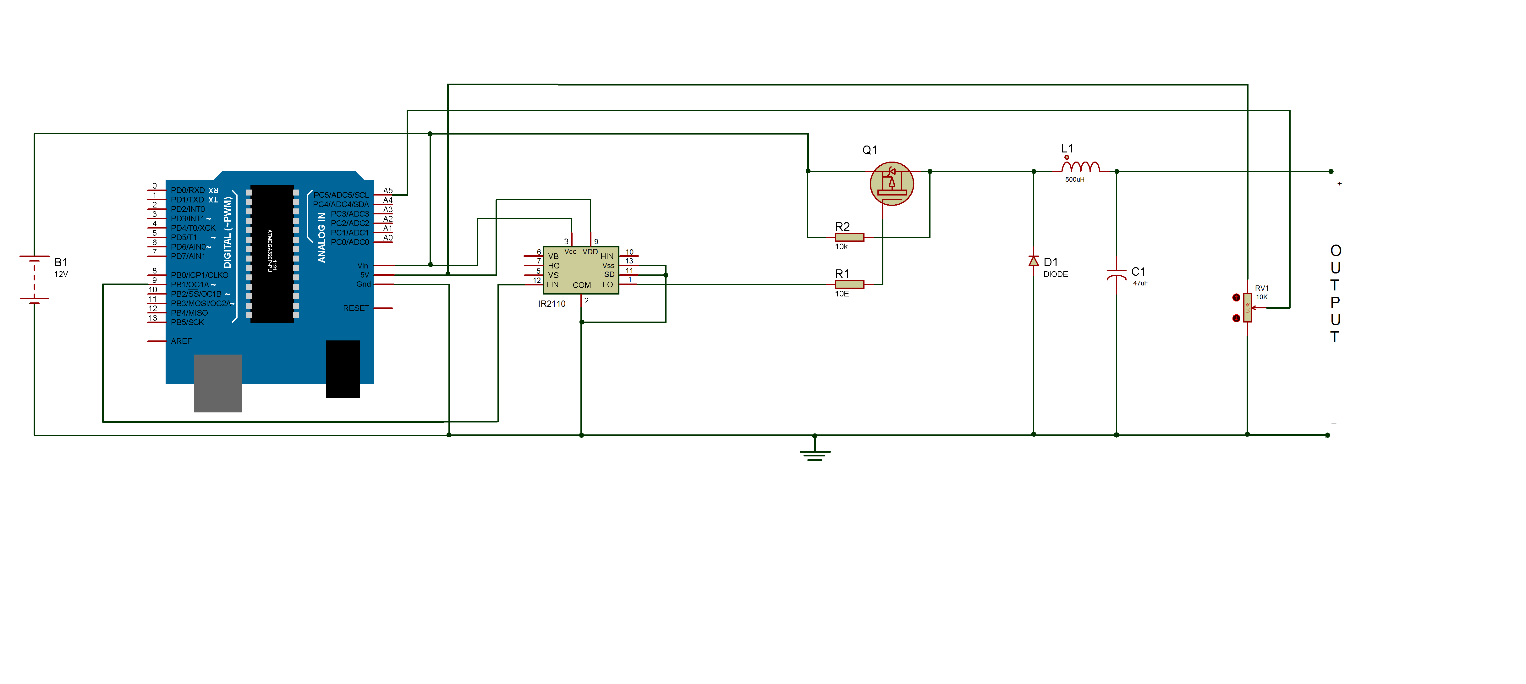
In this tutorial, a non-isolated buck converter is designed which means the input and output share the same ground. The buck converter designed in this project will step down 12V DC to 5V DC with a tolerance limit of +/-0.5 V. The output voltage will be adjustable between 5V and 9V. Once the circuit is designed and assembled, the value of the output voltage and current will be observed using a multimeter. These values will indicate the efficiency of the buck converter designed in the project.
Components Required –

Fig. 1: List of components required for Adjustable Open Loop Buck Converter
Block Diagram –

Fig. 2: Block Diagram of Adjustable Open Loop Buck Converter
Circuit Connections –
In this project, an open loop buck converter operating in CCM mode is designed and the component values as per the CCM standard equations are calculated for the desired output.
The buck converter has the following circuit blocks –
1. DC source –
A 12V Battery is used as the input power source in the circuit.
2. Oscillator and Switching Mechanism –
For switching purpose a transistor and a diode are used as switching components.
The switching components has to operate on a specific frequency. This frequency is generated through an oscillator circuit. In this project, Arduino UNO is used to generate a PWM signal which provides the required frequency. Any other Arduino Board like Arduino Mega can also be used. In fact any microcontroller or microcontroller board which can output PWM can be used in the circuit. Arduino is chosen as it is the most popular prototyping board and can be easily programmed. Due to large community support, it is easy to learn and work on Arduino. The PWM signal is a train of the pulse which is used to turn ON and OFF the MOSFET. The MOSFET is used as the switching transistor in the circuit.
For switching purpose, a transistor and a diode are used as a switching components For the selection of the transistor, MOSFET is chosen as FETs are known for their fast switching speed and low RDS (ON) (drain to source resistance in ON state). In this configuration, the MOSFET is connected in high-side configuration. As in high side, the N-channel MOSFET requires a Bootstrap Circuitry or a Gate Driver IC for its triggering, this makes the driver more complicated. A P-channel MOSFET (shown as Q1 in the circuit diagram) is used in the circuit as it does not require a Gate Driver in its high side but it has high Rds (On) as compared to N-MOS. This results in more power loss. The MOSFET used in the circuit has its threshold voltage around 10V to 12V.
The switching time of the MOSFET and diode should be less than the rise and fall time of the PWM wave. The diode should offer low voltage drop in forward bias and the RDS (ON)of the MOSFET should be low. Always a gate to source resistance should be used to avoid any unwanted triggering of the MOSFET by external noise. It also helps in fast turning OFF the MOSFET by discharging its parasitic capacitance. A low value of the resistor (10E to 500E) can be used at the gate of MOSFET. This will solve the problem of ringing (parasitic oscillations) and inrush current in the MOSFET. The voltage level of the PWM signal should be greater than the threshold voltage of the MOSFET. So that the MOSFET can be turned ON fully with minimum RDS (ON ) .
The MOSFET cannot be triggered by the microcontroller as the microcontroller can generate a 5V PWM signal only. Therefore an additional IC IR2110 is used in the circuit to generate a PWM signal of 12V and the input to the IR2110 is provided by the microcontroller. IR2110 is a high and low side driver. It is a high speed (operational at high frequency) power MOSFET and IGBT driver with independent high and low side referenced output channels. The floating channels can operate up to 500V or 600 V. The IC is 3.3V logic compatible that is why it can be used with any microcontroller. The IC comes in a 14 Lead PDIP package.
IR2110 has the following pin configuration –

Fig. 3: Table listing pin configuration of IR2110 IC
Another switching component used in the circuit is a diode. The switching time of the diode should be less than the rise and fall time of the PWM wave. The Arduino board generates a PWM wave having rise time 110ns and fall time of 90ns. The forward voltage drop of the diode should also be very low otherwise it will dissipate power which will further reduce the efficiency of the circuit. The diode should offer low voltage drop in forward bias and the RDS (ON)of the MOSFET should be low. So in this experiment, a BY399 diode is selected which suits best to the circuit design.
Before generating the PWM signal the switching frequency for the circuit needs to be decided. For this buck converter, a switching frequency of 20kHz is selected which will work fine for this converter design.
The duty cycle of the generated PWM signal is another important consideration as it will decide the active state of the MOSFET. The duty cycle can be calculated as follows –
For minimum output voltage, Vout = 5V,
Duty Cycle, D% = (Vout/Vin)*100
Desired output voltage, Vout = 5V
Input voltage, Vin = 12V
By putting all the values,
Dmin% = 40% (approx.)
For maximum output voltgae,Vout = 9V,
Duty Cycle, D% = (Vout/Vin)*100
Desired output voltage, Vout = 9V
Input voltage, Vin = 12V
By putting all the values,
Dmax% = 75% (approx.)
For generating 20 kHz PWM signal with 40% to 75% duty cycle, the Arduino board is programmed. The Arduino sketch required for generating the desired PWM output is attached in the tutorial. It can be downloaded and burnt to an Arduino board for use.
The higher is the frequency selected for switching components, the higher are the switching losses. This decreases the efficiency of the SMPS. But high switching frequency reduces the size of the energy storage element and improves the transient response of the output.
3. Energy Storage Element –
An inductor is used for storing the electrical energy in the form of magnetic field. So the inductor acts like an Energy Storage Element. An inductor of 500 uH value is used in the circuit. For an inductor, a transformer’s secondary or primary coil, relay coil or any standard inductor can be used which has the desired inductance value. The value of inductor can be calculated by the standard equation of CCM as follows –
Lmin>=(Vout *(1-Vout/Vin))/(Fs*2*Io(critical))
Where,
Lmin = minimum value of inductor
Desired output voltage, Vout = 5V
Input voltage, Vin = 12V
Switching frequency, Fs = 20kHz
Io (min) = Critical value of output current to maintain a regulated voltage at the output.
As inductor value depend on critical current, so first value of Io(critical) should be calculated as follow –
Io(critical) = ((Vin – Vout)*D*Ts)/(2*L)
From the above equations it can be analyzed that the ‘L’ and ‘Io’(critical) are dependent on each other so either of the two values should be assumed. In this experiment, the value of inductor is assumed to be 500 uH. Now, the value of critical current can be calculated as follow –
Assuming L = 500uH,
For Vout = 5V, Io(critical) is –
Io(critical) = ((Vin – Vout)*Dmin*Ts)/(2*L)
Io(critical) = ((12 – 5)*0.4*50*10-6)/(2*500*10-6)
Io(critical) = 140mA
For Vout = 9V, Io(critical) is –
Io(critical) = ((Vin – Vout)*Dmax*Ts)/(2*L)
Io(critical) = ((12 – 9)*0.75*50*10-6)/(2*500*10-6)
Io(critical) = 112mA
The inductor current rating should be greater than the inductor ripple current so that the desired current at the output can be obtained.
4. Output Filtering Element –
As a filtering element, a capacitor (shown as C1 in the circuit diagram) is used at the output of the circuit. In normal operation of Buck converter circuit, the transistor Q1 turns ON and OFF according to the frequency of the oscillator circuit. This generates a train of the pulse at the inductor L1 and capacitor C1 as well as transistor Q1. As the capacitor is connected with inductor in both negative and positive cycle of the PWM signal. This makes an LC filter which filters the train of the pulse to produce a smooth DC at the output. The value of the capacitor can be calculated by using following equation of CCM –
Cmin >= DIL/(8*Fs*DVo)
Where,
Cmin = minimum value of capacitor
DIL=Inductor ripple current
DVo = Output ripple voltage
Assuming DVo = 100mV
Now for calculating DIL,
DIL= 2*Io(critical)
DIL= 2*140*10-3
DIL= 280mA
By putting all the value,
Cmin >= (280*10-3)/(8*20*103*100*10-3)
Cmin >= 18uF
As it is the minimum value of capacitor required, so in the circuit a capacitor of standard value is used which can be easily available, so, capacitor of 47uF is taken.
The value of the capacitor should be greater than or equivalent to the calculated value. So that it is able to provide the desired current and voltage at the output. The capacitor used in the circuit must be of higher voltage rating than the output voltage. Otherwise, the capacitor will start leaking the current due to the excess voltage at its plates and will burst out. It is important that all the capacitors should be discharged before working on a DC power supply application. For this, the capacitors should be shorted with a screwdriver wearing insulated gloves.
5. Output Voltage Adjustment –
For varying the output voltage a potentiometer is used at the output of the circuit (as shown in the circuit diagram). The potentiometer gets powered by the 5V supply of the Arduino board and then the analog pin of microcontroller sense the voltage of the potentiometer. After sensing the voltage, the microcontroller adjusts the duty cycle as per the desired output voltage. So by turning the knob of potentiometer, the output voltage can be varied as per the requirement.
How the Circuit works –
Any SMPS has some switching components which turn on and off at high frequency and has some storage component which store the electrical energy while the switching components are in conduction state and discharge the stored energy to the output device while the switching components are in non-conduction state.
A simple Buck Converter consists of the inductor (L1), a diode (D1), a capacitor(C1) and a transistor which acts like a switch. Initially when the switch is open then the current in the circuit is zero. When for the first time the switch is closed then the inductor opposes the change in current and produces an opposing voltage at its terminal. This makes the diode reverse biased. The voltage drop across inductor counteracts the source voltage which results in less voltage at the output. When time elapses the rate of change of current decreases and the voltage drop across the inductor also decreases. In this state, the inductor starts storing energy in the form of magnetic field. The output capacitor is charged throughout the ON state. The stored charged in the capacitor provides the required current to the load in OFF state.

Fig. 4: Circuit Diagram showing ON state of switching Component in Buck Converter
When the switch opens, the input source is disconnected from the circuit and the current starts decreasing and becomes zero. As the inductor has stored energy in the previous cycle, it now acts as an energy source. Hence, the inductor creates a polarity across it. This is opposite in polarity as in the ON state. This makes the diode forward biased and the inductor now provides the current to the load through diode D1. When the stored charge in inductor starts reducing then the output voltage starts falling. Now the capacitor acts as a current source and keeps providing the current to the load until the next cycle i.e. ON state. The overall effect is that at the output a small DC voltage with high output current is obtained as compared to the input.

Fig. 5: Circuit Diagram showing OFF state of switching Component in Buck Converter
In the ON state, the Diode was in blocking Mode (OFF) and the Transistor was ON. In OFF state, the Diode was in conducting mode (ON) and the Transistor was OFF. So, a Buck Converter is having two switches, one is a transistor and another one is the diode. At a time only one of them conducts while other goes in non-conduction state.
As a variable resistor is used to draw output, the output voltage can be varied within the desired range. The component values are already calculated considering the range of voltage required at the output.
Testing the Circuit –
This buck converter has been designed to step down 12V DC to 5V DC.

Fig. 6: Prototype of Open Loop Buck Converter designed on a breadboard
In this circuit, Input Voltage, Vin = 12V
Practically, Battery Voltage, Vin = 11.8V
On measuring voltage and current values with different loads at the output when duty cycle is set to 40 percent, following observations were taken –

Fig. 7: Table listing output voltage and current from Adjustable Open Loop Buck Converter for different loads at 40 percent Duty Cycle
So, it can be observed that a maximum current of 145 mA can be drawn at output with a tolerance limit of +/-0.5V when duty cycle is set to 40%.
On measuring voltage and current values with different loads at the output when duty cycle is set to 75 percent, following observations were taken –

Fig. 8: Table listing output voltage and current from Adjustable Open Loop Buck Converter for different loads at 75 percent Duty Cycle
So, it can be observed that a maximum current of 120 mA can be drawn at output with a tolerance limit of +/-0.5V when duty cycle is set to 75%.
The power efficiency of the circuit at maximum output current of 145 mA and output voltage at 4.52 V can be calculated as follows –
Efficiency % = (Pout/Pin)*100
(Output Power) Pout = Vout*Iout
(Output voltage),Vout = 4.52V
(Output current) Iout = 145mA
Pout = 655mW (approx.)
(Input Power) Pin = Vin*Iin
(Input voltage) Vin = 11.8V
(Input Current) Iin = 70mA
Pin = 11.8 *0.07
Pin = 826mW (approx.)
By putting all the values,
Efficiency % = (655/826)*100
Efficiency % = 80% (approx.)
It can be seen that there are certain limitations of this circuit. The output voltage in this circuit is not regulated it varies for different load resistances. This can be improved by adding a feedback circuitry which helps in regulating the output voltage. Secondly, the efficiency of this design is less as the power losses in the circuit are not considered. There are switching and conduction losses of diode and MOSFET, losses in the windings that surround the core, eddy current losses and hysteresis losses in the inductor, capacitor losses due to ESR (equivalent series resistance) and losses due to high Rds(on) of P-MOS.
This is an open loop buck converter with non-isolated output and operating in CCM mode. It can be used as a low loss current source to drive LEDs or power portable self-powered devices. It can also be used as an interface between battery and components in CPU or notebooks where voltage demand is lower than battery voltage.
Project Source Code
###
//Program toCode for Buck Converter with Input voltage = 12V and Adjustable Output voltage = 5V to 9V This code will generate a PWM (Pulse Width Modulation)signal of 20kHz. The output voltage can vary from 5V to 9V by adjusting the duty cycle. */ #define TOP 799 // Fosc = Fclk/(N*(1+TOP)); Fclk = 16MHz, Fosc = 20kHz #define CMP_VALUE_HALF_DUTY 399 // 50% duty cycle #define Inputpin A5 // Input pin of potentiometer at A5 #define PWM 9 // PWM(Pulse Width Modulation) wave at pin 9 float Mapping_output_voltage(); // function declaration float Mapping_output_voltage(){ // function definition int Input_Read = analogRead(Inputpin); //reading analog voltage from potentiometer and converting it to digital values in between 0 to 1023 float Compare_voltage = (((Input_Read*(1.0)/1024)*4)+5); // mapping the digital value into analog voltage of 5V to 9V return(Compare_voltage); // return the calculated output voltage } void setup() { // put your setup code here, to run once: pinMode(PWM,OUTPUT); //set 9 pin as output pinMode(Inputpin,INPUT); // set A5 pin as input TCCR1A = 0; //reset the register TCCR1B = 0; //reset the register TCNT1 = 0; //reset the register TCCR1A |= (1<<COM1A1); // set output at non inverting mode TCCR1A |= (1<<WGM11); // selecting Fast PWM(pulse width modulation) mode ICR1 = TOP; // setting frequency to 20KHz TCCR1B |= (1<< CS10)|(1<<WGM12)|(1<<WGM13); //Timer Starts OCR1A = CMP_VALUE_HALF_DUTY; // setting PWM of 50% duty cycle delay(1000); // delay for compensating the hardware transient time with software } void loop() { // put your main code here, to run repeatedly: float Output_voltage = Mapping_output_voltage(); // getting desired output voltage float Desired_Duty_cycle = (1-(Output_voltage/12)); //calculating duty cycle as per the desired output voltage int OCR_value = (799*Desired_Duty_cycle); //calculating OCR1A values as per the desired duty cycle OCR1A = OCR_value; // updating OCR1A register as per the desired duty cycle }###
Circuit Diagrams
Project Video
Filed Under: Electronic Projects
Filed Under: Electronic Projects

Questions related to this article?
👉Ask and discuss on Electro-Tech-Online.com and EDAboard.com forums.
Tell Us What You Think!!
You must be logged in to post a comment.