The PWM is a technique which is used to drive the inertial loads since a very long time.The simple example of an inertial load is a motor. Apply the power to a motor for a very short period of time and then turn off the power: it can be observed that the motor is still running even after the power has been cut off from it. This is due to the inertia of the motor and the significance of this factor is that the continuous power is not required for that kind of devices to operate. A burst power can save the total power supplied to the load while achieving the same performance from the device as it runs on continuous power.
The PWM technique is use in devices like DC motors, Loudspeakers, Class -D Amplifiers, SMPS etc. They are also used in communication field as-well. The modulation techniques like AM, FM are widely used RF communication whereas the PWM is modulation technique is mostly used in Optical Fiber Communication (OFC).
As in the case of the inertial loads mentioned previously, the PWM in a communication link greatly saves the transmitter power. The immunity of the PWM transmission against the inter-symbol interference is another advantage. This article discusses the technique of generating a PWM wave corresponding to a modulating sine wave.
DESCRIPTION:
The Pulse Width Modulation is a technique in which the ON time or OFF time of a pulse is varied according to the amplitude of the modulating signal, keeping t
")
Fig. 1: Block Diagram of Pulse Width Modulation (PWM)
he (ON time + OFF time) time of the pulse as constant. The (ON time + OFF time) of a pulse is called ‘Period’ of the pulse, and the ratio of the ON time or OFF time with the Period is called the ‘Duty Cycle’. Hence the PWM is a kind of modulation which keeps the Period of pulses constant but varying their duty cycle according to the amplitude of the modulating signal.
The conventional method of generating a PWM modulated wave is to compare the message signal with a ramp waveform using a comparator. The block diagram required for the generation of a simple PWM is shown in the following:
1) Variable frequency sine wave generator
A sine wave generator circuit is used in this project which is based on the Wien Bridge Oscillator (WBO) circuit. The Wien Bridge oscillator circuit can produce distortion less sinusoidal sweep at its output. The circuit is designed in such a way that both the amplitude and frequency of the oscillator can be adjusted using potentiometers.
The circuit diagram of the variable frequency sine wave oscillator is shown in the following:

Fig. 2: Circuit Diagram of Variable Frequency Sine Wave Oscillator

Fig. 3: Variable Frequency Sine Wave Oscillator Circuit on Breadboard
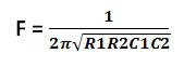
The frequency of the above circuit can be varied by simply varying the potentiometer R2 and the amplitude of the wave form can be adjusted by varying the potentiometer R. The frequency of the sine wave generated by the above circuit depends on the components R1, R2, C1 and C2 and the equation for the frequency is given below:
For the ease of adjusting the amplitude of the wave to obtain proper sinusoidal sweep, a coarse and fine adjustment has been implemented using potentiometers. A low value (1K) potentiometer is connected in series with the high value (100K) potentiometer so that the coarse adjustment can be done with the high value resistor and the fine adjustment with the low value resistor.
The snapshot of the waveform formed at the CRO screen using the WBO circuit is shown in the following image:

Fig. 4: Sine Waveform on CRO Screen using Wien Bridge Oscillator Circuit
2) Ramp generator
The Ramp generator used in this circuit is designed with an op-amp and an RC charging circuit. The RC charging circuit is connected to the output of the op-amp and the voltage across the capacitor is connected to one of the input of the op-amp. To another input of the op-amp the variable pin of a potential divider is connected to which divides the voltage from the output of the op-amp.

Fig. 5: Circuit Diagram of Ramp Generator
The op-amp here acts as a simple comparator and the potential divider is used to set the threshold of comparison. As the capacitor charges through the output potential of the op-amp (either 5V or -5V), the voltage across the capacitor increases. At some point the voltage across the capacitor becomes greater than which has been set using the potentiometer and as a result the output voltage of the comparator changes. It forces the capacitor to discharge immediately. The capacitor charges slowly through a resistor, but it discharges immediately through a diode which conducts only when the current flows in the discharging direction. Due to this slow charging and very fast discharging the voltage across the capacitor appears like a ramp waveform. The image of the circuit wired in the bread board is shown in the following figure:

Fig. 6: Ramp Generator Circuit on Breadboard
The frequency of the ramp wave depends on the charging period of the RC circuit. The charging period depends on the RC constant which is the product of the values of the Resistance and the Capacitance.
Time period of the ramp,
Tramp = R * C
The image captured from the CRO screen displaying a ramp waveform is shown below:

Fig. 7: Ramp Waveform on CRO Screen
Comparator Circuit
3) Comparator
The ramp waveform is applied to one of the input of another comparator circuit and the output of the comparator circuit will be a PWM waveform. The comparator circuit is shown in the following figure:

Fig. 8: Circuit Diagram of Comparator
The image of the circuit wired on the breadboard is shown below:
Fig. 9: Comparator Circuit on Breadboard
The following is the image captured from the CRO screen displaying the PWM waveform:
Fig. 10: PWM Waveform on CRO Screen
The complete circuit diagram is given below:
Fig. 11: Circuit Diagram of Pulse Width Modulation (PWM)
The 1M ohm resistor is used to adjust the amplitude of the sine wave signal generated by the WBO. The amplitude of the sine wave should be adjusted in such a way that it matches with the amplitude of the ramp signal generated.
The image of PWM circuit wired in the breadboard is given below:

Fig. 12: PWM Circuit on Breadboard
Filed Under: Circuit Design

Questions related to this article?
👉Ask and discuss on Electro-Tech-Online.com and EDAboard.com forums.
Tell Us What You Think!!
You must be logged in to post a comment.