Engineers Garage

  • Electronics Projects and Tutorials
    • Electronic Projects
      • Arduino Projects
      • AVR
      • Raspberry pi
      • ESP8266
      • BeagleBone
      • 8051 Microcontroller
      • ARM
      • PIC Microcontroller
      • STM32
    • Tutorials
      • Audio Electronics
      • Battery Management
      • Brainwave
      • Electric Vehicles
      • EMI/EMC/RFI
      • Hardware Filters
      • IoT tutorials
      • Power Tutorials
      • Python
      • Sensors
      • USB
      • VHDL
    • Circuit Design
    • Project Videos
    • Components
  • Articles
    • Tech Articles
    • Insight
    • Invention Stories
    • How to
    • What Is
  • News
    • Electronic Product News
    • Business News
    • Company/Start-up News
    • DIY Reviews
    • Guest Post
  • Forums
    • EDABoard.com
    • Electro-Tech-Online
    • EG Forum Archive
  • DigiKey Store
    • Cables, Wires
    • Connectors, Interconnect
    • Discrete
    • Electromechanical
    • Embedded Computers
    • Enclosures, Hardware, Office
    • Integrated Circuits (ICs)
    • Isolators
    • LED/Optoelectronics
    • Passive
    • Power, Circuit Protection
    • Programmers
    • RF, Wireless
    • Semiconductors
    • Sensors, Transducers
    • Test Products
    • Tools
  • Learn
    • eBooks/Tech Tips
    • Design Guides
    • Learning Center
    • Tech Toolboxes
    • Webinars & Digital Events
  • Resources
    • Digital Issues
    • EE Training Days
    • LEAP Awards
    • Podcasts
    • Webinars / Digital Events
    • White Papers
    • Engineering Diversity & Inclusion
    • DesignFast
  • Guest Post Guidelines
  • Advertise
  • Subscribe

DIY – Clocked SR Flip Flop

By Ashutosh Bhatt March 6, 2017

SR flip-flop is a short form of set-reset flip-flop. Its output is either set means high (logic 1) or reset means low (logic 0) as per set or reset inputs given. When set input is given logic 1 (high), the flip-flop is set and its Q output is high (another complemented output QBAR will be low) and when reset input is given logic 1, the flip-flop is reset and its Q output is low (QBAR output will be high). In clocked SR flip-flop, the output states will change only when a clock pulse is applied along with S & R inputs.

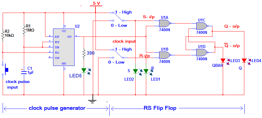
Here, the given circuit demonstrates the operation of clocked SR flip-flop. The flip-flop is built using four 2 input NAND gates and clock pulse generator is built using multivibrator chip IC NE555. SPDT switches are used to give S and R inputs as logic 1 (high – 5 V) and logic 0 (low – 0 V). Different RED and GREEN LEDs are used for input-output logic indications. Please refer the table given below.

Table listing LED Status for Logic Levels of 555 IC based Clocked SR Flip Flop

Fig. 1: Table listing LED Status for Logic Levels of 555 IC based Clocked SR Flip Flop

The circuit is very easy to build and all the components are also easily available and cheap. Here is the list of required components.

List of Components required for 555 IC based Clocked SR Flip Flop

Fig. 2: List of Components required for 555 IC based Clocked SR Flip Flop

The circuit can be built on general purpose PCB or breadboard. So let us see the circuit diagram followed by its description and operation.

CIRCUIT DESCRIPTION

The complete circuit is divided into two different sections -:

1. Clock pulse generator circuit

2. RS flip flop circuit

Clock pulse generator circuit is built using IC NE555. IC NE555 is wired in monostable mode. Timing components R1 and C1 are chosen such as to give pulse output of 1 sec approx. A push button is connected to trigger input pin 2. The output of IC is given as clock pulse input to the flip-flop circuit. One LED is connected (LED5) to this output to indicate clock pulse output from the circuit.

SR flip-flop circuit is built using quad 2 input NAND gate chip 74LS00. The circuit consists of 4 2 input NAND gates, 2 SPDT switches for input and 4 LEDs for indications and outputs. Two SPDT switches provide logic 1 (high) or logic 0 (low) to S and R inputs. The status of S and R inputs is indicated by two green LEDs LED1 and LED2.  The Q and QBAR outputs of the flip-flop are connected to two red LEDs LED3 and LED4 as shown. The complete circuit works on 5 V supply.

Here is the snap of circuit arrangement.

Prototype of 555 IC based Clocked SR Flip Flop

Fig. 3: Prototype of 555 IC based Clocked SR Flip Flop

CIRCUIT OPERATION

Clock pulse generation circuit – because IC NE555 is wired in a monostable mode it will generate 1 sec pulse every time when a trigger input is applied by pressing push button. The LED blinks to indicate clock pulse is generated.

SR flip-flop circuit – The circuit works as per following truth table.

Truth Table of Clocked SR Flip Flop

Fig. 4: Truth Table of Clocked SR Flip Flop

First, S is given logic 1 input and R is given logic 0 input through SPDT switches. Now when the clock pulse is given from clock pulse generator circuit, the two inputs of U1A gate become high (logic 1). So as per NAND gate operation* its output goes low (logic 0). As this output is connected to one input of U1C, the output of U1C becomes high immediately as per NAND gate truth table*. The Q output is high and LED4 glows. This output is given as input to U1D. Another input to U1D is from U1B and that is also high because its input R is low. So now, as both the inputs of U1D are high, its output will go low. Thus QBAR output is low and LED3 is off.

In the second case, S input is given logic 0 and R is given logic 1. When clock input is high, the two inputs of U1B gate become high (logic 1). So its output goes low (logic 0). As this output is connected to one input of U1D, the output of U1D becomes high immediately. The QBAR output is high and LED3 glows. This output is given as input to U1C. Another input to U1C is from U1A and that is also high because its input S is low. So now, as both the inputs of U1C are high, its output will go low. Thus Q output is low and LED4 is off.

Similarly in 3rd case, when both S and R inputs are low, the Q and QBAR outputs will remain as it was previously. There will be no change in Q and QBAR output.As given in the last case, we cannot apply both S and R inputs as high. This will make the outputs of gates U1A and U1B low and this would make outputs of U1C and U1D high. That means Q and QBAR both outputs will be high. And this must not happen. That’s why we cannot apply both S and R inputs high.

*NAND gate truth table

Truth Table of NAND Gate

Fig. 5: Truth Table of NAND Gate


Circuit Diagrams

Circuit-Diagram-555-Ic-Based-Clocked-SR-Flip-Flop

Project Video


Filed Under: Electronic Projects


Next Article

← Previous Article
Next Article →

Questions related to this article?
👉Ask and discuss on EDAboard.com and Electro-Tech-Online.com forums.


Tell Us What You Think!! Cancel reply

You must be logged in to post a comment.

EE TECH TOOLBOX

“ee
Tech Toolbox: Internet of Things
Explore practical strategies for minimizing attack surfaces, managing memory efficiently, and securing firmware. Download now to ensure your IoT implementations remain secure, efficient, and future-ready.

EE Learning Center

EE Learning Center
“engineers
EXPAND YOUR KNOWLEDGE AND STAY CONNECTED
Get the latest info on technologies, tools and strategies for EE professionals.

HAVE A QUESTION?

Have a technical question about an article or other engineering questions? Check out our engineering forums EDABoard.com and Electro-Tech-Online.com where you can get those questions asked and answered by your peers!


RSS EDABOARD.com Discussions

  • How can I get the frequency please help!
  • Elektronik devre
  • 12VAC to 12VDC 5A on 250ft 12AWG
  • SPI speed pic18f66j15
  • Antiparallel Schottky Diodes VDI-Load Pull

RSS Electro-Tech-Online.com Discussions

  • how to work on pcbs that are thick
  • compatible eth ports for laptop
  • How to repair this plug in connector where wires came loose
  • Actin group needed for effective PCB software tutorials
  • Kawai KDP 80 Electronic Piano Dead

Featured – Designing of Audio Amplifiers part 9 series

  • Basics of Audio Amplifier – 1/9
  • Designing 250 Milli Watt Audio Power Amplifier – 2/9
  • Designing 1 Watt Audio Power Amplifier – 3/9
  • Designing a Bass Boost Amplifier – 4/9
  • Designing a 6 Watt Car Audio Amplifier – 5/9
  • Design a low power amplifier for headphones- 6/9

Recent Articles

  • ITG Electronics releases gate drive transformers with 200 – 450 V DC capability
  • Stackpole introduces HCJ jumpers with 70.7 amp continuous current capability
  • Infineon releases MCU with 128K flash and multi-sense capabilities
  • ST introduces 600V GaN gate drivers with 300 ns start-up time
  • ABLIC releases S-19116 automotive voltage detector with 6.8μs response time

EE ENGINEERING TRAINING DAYS

engineering

Submit a Guest Post

submit a guest post
Engineers Garage
  • Analog IC TIps
  • Connector Tips
  • Battery Power Tips
  • DesignFast
  • EDABoard Forums
  • EE World Online
  • Electro-Tech-Online Forums
  • EV Engineering
  • Microcontroller Tips
  • Power Electronic Tips
  • Sensor Tips
  • Test and Measurement Tips
  • 5G Technology World
  • Subscribe to our newsletter
  • About Us
  • Contact Us
  • Advertise

Copyright © 2025 WTWH Media LLC. All Rights Reserved. The material on this site may not be reproduced, distributed, transmitted, cached or otherwise used, except with the prior written permission of WTWH Media
Privacy Policy

Search Engineers Garage

  • Electronics Projects and Tutorials
    • Electronic Projects
      • Arduino Projects
      • AVR
      • Raspberry pi
      • ESP8266
      • BeagleBone
      • 8051 Microcontroller
      • ARM
      • PIC Microcontroller
      • STM32
    • Tutorials
      • Audio Electronics
      • Battery Management
      • Brainwave
      • Electric Vehicles
      • EMI/EMC/RFI
      • Hardware Filters
      • IoT tutorials
      • Power Tutorials
      • Python
      • Sensors
      • USB
      • VHDL
    • Circuit Design
    • Project Videos
    • Components
  • Articles
    • Tech Articles
    • Insight
    • Invention Stories
    • How to
    • What Is
  • News
    • Electronic Product News
    • Business News
    • Company/Start-up News
    • DIY Reviews
    • Guest Post
  • Forums
    • EDABoard.com
    • Electro-Tech-Online
    • EG Forum Archive
  • DigiKey Store
    • Cables, Wires
    • Connectors, Interconnect
    • Discrete
    • Electromechanical
    • Embedded Computers
    • Enclosures, Hardware, Office
    • Integrated Circuits (ICs)
    • Isolators
    • LED/Optoelectronics
    • Passive
    • Power, Circuit Protection
    • Programmers
    • RF, Wireless
    • Semiconductors
    • Sensors, Transducers
    • Test Products
    • Tools
  • Learn
    • eBooks/Tech Tips
    • Design Guides
    • Learning Center
    • Tech Toolboxes
    • Webinars & Digital Events
  • Resources
    • Digital Issues
    • EE Training Days
    • LEAP Awards
    • Podcasts
    • Webinars / Digital Events
    • White Papers
    • Engineering Diversity & Inclusion
    • DesignFast
  • Guest Post Guidelines
  • Advertise
  • Subscribe