Step: 5) Design circuit for each functional block
In this step we will be designing the circuit for individual blocks. The circuits required are simple and very basic circuit known to all; hence it won’t be such a big task. We are not designing anything new, but modifying the well-known basic circuits to suit our needs.
Let us begin with the IR sensing part itself as we have done in the case of the block diagram. In the IR sensing part we have two blocks namely the IR PHOTODIODE and the COMPARATOR.
IR PHOTODIODE:
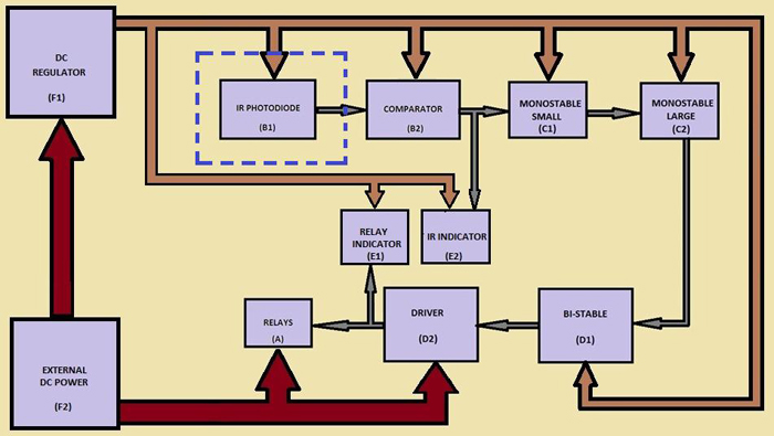
Fig. 1: Functional Block Of IR Photodiode
We can use any commonly available IR photodiode to realize this block. All we need is a pull-down resistor with its output. The pull-down resistor is used to set a default output when there is no IR light falling on the photodiode.
IR photodiode is a PN junction diode whose depletion region width (kindly refer any basic electronic text book) is sensitive to the incoming IR light rays. It acts very much like a normal diode in the forward biased condition. In reversed biased condition when there is no IR light the depletion region width increases and the conduction decreases as in the case of the normal diodes. But when the IR light falls on the depletion region, reverse breakdown occurs, depletion region width decreases and the conduction increases considerably. The conduction current in certain ranges is proportional to the incoming IR light.
We can make use of this phenomenon in our design. Connect the IR photodiode in reverse biased configuration and take the output from one of its legs. Such a circuit is shown in the following figure
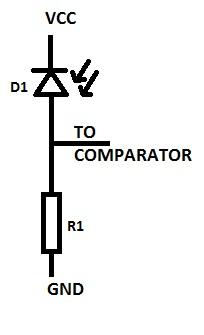
Fig. 2: IR Photodiode Circuit
As you can see from the above circuit that the ‘D1’ which is the IR photodiode is connected in reverse biased. Output is taken at the positive lead of the photodiode. Whenever light falls on the IR photodiode it conducts and we get a positive voltage at the output which depends on the intensity of the IR light falling on it.
The resistor R1 is used as a pull down resistor. It is used to set a default output voltage when there is no light falling on the photodiode. What will be the voltage at the output if there is no IR light falling on the photodiode and when there is no resistor R1? The answer is there is no voltage, not even zero or ground. But we are expecting a zero voltage when there is no IR light, hence if we connect a resistor to ground and take the output from the point where the photodiode is connected with the resistor we will get a zero voltage.
The resistor R1 is used not only as a pull down resistor but it biases the photodiode in such a way that the photodiode operates only in a limited current when the conduction occurs in reverse biased condition due to the IR light.
Since we will be using the TV remote from a distance the IR light intensity falling on the photodiode will be very small. We must get a strong output from this block even at this less intense IR light. Since for less intense IR light the photodiode current will be less also, we need to amplify the output using this current.
We all know Ohm’s law; it states that “at a given temperature the voltage across a current conducting material is directly proportional to the current flowing through it”. The proportionality constant is nothing but the resistance of the material.
V = IR (Equation: 4)
Where;
‘V’ is the voltage across the current conducting material
‘I’ is the current flowing through the material
‘R’ is the resistance of the material
We can make use of the Equation: 4 in our design. We are taking the output across the resistor R1 and according to Ohm’s law as we increase the resistance we get more voltage across the resistor for a given current flowing through it.
Since the current flowing through the photodiode depends on the intensity of the IR light falls on it we have values ranging between zero and five volts at the output of this circuit.
|
SUPPLY VOLTAGE |
5V DC REGULATED |
|
OUTPUT VOLTAGE |
BETWEEN 0 and 5 VOLTS |
Fig. 3: IR PHOTODIODE Voltages
For a significant output voltage even for the weakest signal, we must use a resistor with the high resistance. We can use a 100K resistance as the resistor R1.
The photodiode D1 can be any common photodiode and I’ve used “glass type Directional IR Photodiode” which is commonly called “IR LED receiver”. I don’t have the part number, but the image of the same is given below.
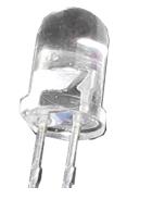
Fig. 4: IR Photodiode
The component used in the IR PHOTODIODE circuit and their functions are given in the following table
|
COMPONENT |
FUNCTION |
|
D1 |
The photodiode for sensing the incoming IR light rays |
|
R1 |
The resistor acts as a pull down resistor with the photodiode and is used for biasing the photodiode. Increases the resistance will increase the sensitivity up to certain extend. |
Fig. 5: IR PHOTODIODE Component Functions
The components designed for this particular block of circuit is given in the table below.
|
Serial no. |
COMPONENT |
TYPE |
VALUE |
|
1 |
D1 |
IR Photodiode |
directional IR photodiode |
|
2 |
R1 |
Resistor |
100KE |
Fig. 6: IR PHOTODIODE Component Values
We have done with the IR PHOTODIODE block and now let us take the COMPARATOR block and try to design the circuit for it.
Circuit Designing Contd
COMPARATOR:
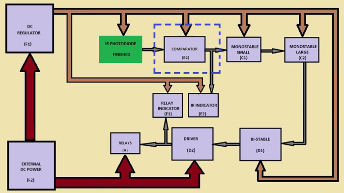
Fig. 7: Functional Block Diagram of Comparator
The comparator module is used to produce an output whenever the output of the IR PHOTODIODE block rises above a particular level. The comparator module basically compare its input which is getting from the IR PHOTODIODE with a voltage and produces a high voltage at the output whenever the input voltage is above the voltage level with which it is compared. We call this technique simply as ‘Level detection’.
The most suitable component for level detection is an op-amp. The op-amp stands for ‘Operational Amplifier’. The op-amp is electronic amplifier circuit whose gain can be adjusted externally. The gain is ideally infinite by default and with the help of external components we can adjust this gain so that the op-amp can be used for our specific purpose. The gain of an op-amp is increased or decreased by using positive or negative feedback circuit respectively.
Another feature of the op-amp is that it has two input leads and we can apply separate voltages or signals on these two pins. The op-amp takes the difference of these voltages and produces an amplified output of that difference voltage.
The symbolic representation of an op-amp is shown below.
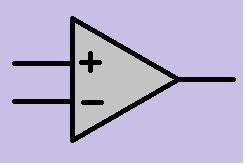
Fig. 8: Symbolic Representation Of Op-Amp
The above figure shows the symbol of an op-amp with two inputs and an output. The leads marked as ‘+’ and ‘-’ are input pins and the other pin is the output pin. The ‘+’ pin is the positive input pin which is used for the positive feedback and the lead marked as ‘-’ is the negative input pin and is used for negative feedback.
When there is no feedback applied to the positive input or negative input pin the gain of the op-amp is ideally infinity. In such a condition a slight increase in voltage at the positive pin compared to the voltage at the negative pin will raise the output towards the positive maximum voltage and a slight increase in the voltage at the negative pin compared to the positive pin will lower the output towards the negative maximum. This feature of the op-amp makes it useful for the purpose of the level detection.
The voltage level which we intend to be detected is applied on either of the input pins and the voltage to be detected is applied on the other pin. In this case we are going to apply the voltage level on the negative input pin and the voltage to be detected on the positive input pin. Whenever the input voltage applied on the positive pin slightly rises above the voltage on the negative pin the output suddenly rises to the positive maximum and remains positive until the input voltage falls below the level to be detected.
This concept is shown in the following diagram.

Fig. 9: Op-Amp Comparator Waveform
The voltage level on the negative input pin can be set by using a potential divider set up. A potential divider is nothing but two resistors connected back to back and the free end of both the resistors is connected across the voltage to be divided and the output is taken from the point at which one resistor joins the other one. Such a resistor set up is shown in the following figure.
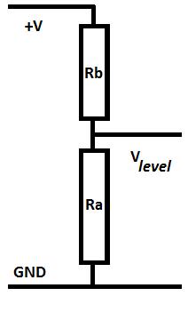
Fig. 10: Potential Divider
In the above figure, two resistors ‘Ra’ and ‘Rb’ are connected across a voltage ‘V’ and an output voltage ‘Vlevel’ is taken from the point where the ‘Ra’ and ‘Rb’ join together. For such a configuration the output voltage ‘Vlevel’ is given as,
Vlevel = V * (Ra / (Ra + Rb)) (Equation: 5)
Where;
(Ra / (Ra + Rb)) is the factor by which the input voltage ‘V’ is divided
This is how a voltage is obtained for setting the voltage level at one of the input pin of the op-amp. In our case we can’t fix a value at the negative input pin since we may have to adjust the value according to the room condition. Hence we are not going to design a potential divider based on the Equation: 5, rather we simply use a variable resistor for the purpose. The two ends of the variable resistor are connected across the supply voltage and the output is taken across the variable lead and the ground.
A circuit using such a variable resistor and the potential divider is shown in the following figure

Fig. 11: Circuit With Variable Resistor And Potential Divider
In the above circuit diagram ‘R2’ is a variable resistor and we can use a 10K variable resistor for this purpose. The value of the total resistance doesn’t matter much since we can vary the resistance according to our need.
The ‘U2’ is an op-amp IC and we are using a LM358 op-amp IC in our circuit. LM358 is a dual op-amp IC, which means it has two op-amps inside it and we can use both of them separately. It is specifically designed to be used with single power supply while most of the op-amps require a dual power supply. The LM358 is widely used for comparator purpose. This IC comes in 8 pin DIP package. The pin-out of a LM358 is shown below.
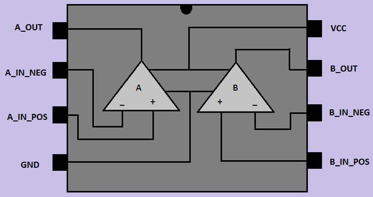
Fig. 12: Pin-Out oof A LM358
The pin description for the 8 pin LM358 is given in the following table
|
PIN NUMBER |
PIN |
DESCRIPTION |
|
1 |
A_OUT |
The output pin of the op-amp A |
|
2 |
A_IN_NEG |
The negative input pin of the op-amp A |
|
3 |
A_IN_POS |
The positive input pin of the op-amp A |
|
4 |
GND |
The ground pin common for both the op-amp A and op-amp B |
|
5 |
B_IN_POS |
The positive input pin for the op-amp B |
|
6 |
B_IN_NEG |
The negative input pin for the op-amp B |
|
7 |
B_OUT |
The output pin for the op-amp B |
|
8 |
VCC |
The VCC pin common for both the op-amp A and op-amp B |
Fig. 13: LM358 Pin Description
If you take a look at the complete block diagram for the design you can see that the COMPARATOR block’s output is not only connected to the MONOSTABLE SMALL block but also to the IR INDICATOR block. We can connect the input pin of another op-amp with the output of IR PHOTODIODE block and with the voltage level set by the resistor R2. The output of that op-amp can be used for the IR INDICATOR block. The COMPARATOR circuit with the IR indicator output is shown in the following figure.
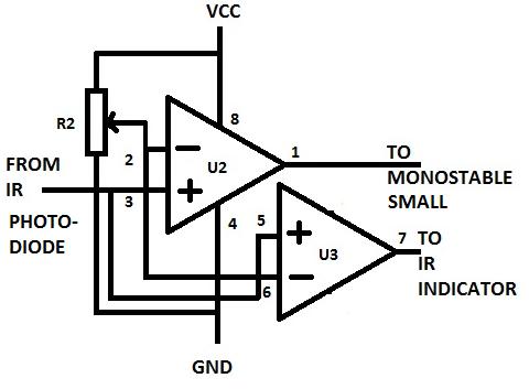
Fig. 14: Comparator Circuit With IR Indicator Output
The component used in the IR PHOTODIODE circuit and their functions are given in the following table
|
COMPONENT |
FUNCTION |
|
R2 |
This is a variable resistor and is use to set the voltage level above which the voltage from the IR PHOTODIODE block needed to be detected by the op-amps. |
|
U2 |
This op-amp is used for the level detection of input from the IR PHOTODODE block and produces an output for the MONOSTABLE SMALL block. It compares the voltage from the IR PHOTODIODE block and whenever the voltage is above the voltage level set by the resistor R2, the output become high |
|
U3 |
This op-amp is used for the level detection of input from the IR PHOTODODE block and produces an output for the IR INDICATOR block. It compares the voltage from the IR PHOTODIODE block and whenever the voltage is above the voltage level set by the resistor R2, the output become high |
Fig. 15: Component Significance Of COMPARATOR Circuit
The component designed for this particular block of circuit is given in the table below.
|
Serial no. |
COMPONENT |
TYPE |
VALUE |
|
1 |
R2 |
Variable resistor |
10KE |
|
2 |
U2 |
Op-amp |
½ LM358 |
|
3 |
U3 |
Op-amp |
½ LM358 |
Fig. 16: COMPARATOR Component Values
The “1/2 LM358” is given in the specification since there is two op-amps in an LM358 IC.
We have finished the design for the COMPARATOR block and now let us move on to the next block which is the MONOSTABLE SMALL block.
Designing Multivibrators
MONOSTABLE SMALL
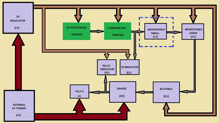
Fig. 17: Functional Block of Monostable Small
We are expecting the MONOSTABLE SMALL block to be a mono-stable circuit with a small quasi-stable time period. The working of the mono-stable multi-vibrator is very much similar to that of a comparator or a level detector. We have a voltage level set inside the mono-stable circuit using a potential divider set up as in the case of a level detector. I contrast to the level detector the voltage to be level detected is generated inside the mono-stable circuit itself. This voltage slowly increases towards the voltage level to be detected and consumes a fixed period of time before crossing the voltage level. Such a voltage source can be generated within the mono-stable circuit using a RC network.
The R-C network is a set up that is used in the circuit to generate a time delay and it can be called a timing circuit, tank circuit etc. The R-C network must include at least a resistor and a capacitor. This resistor and capacitor can be connected in serial or parallel configurations. When a voltage is applied across the R-C network the capacitor charges towards that voltage with a time delay which depends on the value of that resistor and capacitor.
In this circuit we are going to use a series R-C network as shown in the following figure.
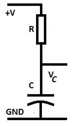
Fig. 18: R-C Network
The R-C network shown in the above figure is made up of a resistor ‘R’ and a capacitor ‘C’ and the circuit is applied across a voltage ‘V’ and the output voltage ‘Vc’ is taken across the capacitor and the ground.
Suppose if the time taken for the circuit to generate an output voltage ‘Vc’ is ‘T’, then the following equation relates the input voltage ‘V’, resistance ‘R’, capacitance ‘C’, time period ‘T’ and the final output voltage ‘Vc’.
Vc = V (1-e-T/RC) (Equation: 6)
Where;
The product RC is called the time constant of the R-C circuit. Simply this is the factor with which the input voltage is delayed to be completely reflected at the output.
Now suppose we need only half of the input voltage at the output, ie. Vc = V/2. The time taken for the output to reach the half of the input voltage can be found out from the Equation: 6 and is given below.
T = 0.693RC (Equation: 7)
As we have mentioned before we are going to apply this timely increasing voltage on one of the input pin of an op-amp and level detect the same voltage using another voltage level fixed at the other input pin. We can use a potential divider for setting the voltage level for detection at one of the input pin of an op-amp. The potential divider set up using two resistors is shown below.
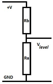
Fig. 19: Potential Divider Set Up For Mono-Stable
Suppose we have applied the fixed voltage level at the positive pin and the timely increasing voltage at the positive input pin then whenever the voltage rises above the level to be detected the output of the op-amp changes. The operation is shown in the following figure.
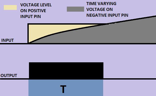
Fig. 20: Level Detection Of R-C Output
As you can see from the above figure that the voltage at the negative input pin due to the capacitor charging process in the R-C network was initially below the voltage level set at the positive input pin and hence the output was high. The voltage at the negative input pin slowly rises towards the input voltage and finally after a time period ‘T’ the voltage at the negative input pin becomes slightly higher than the voltage level at the positive input pin. At this point since the voltage at the negative input pin is higher than the positive input pin the output become low or zero.
The circuit diagram in which the above discussed method has been implemented is shown below.
Figure:
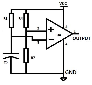
Fig. 21: Circuit Diagarm of R-C Network
In the above shown circuit the resistors R4 and R7 forms the potential divider network and the resistor R3 together with the capacitor C5 forms the R-C network. The ‘U4’ is the op-amp and the positive input is connected to the voltage level set by the potential divider and the negative pin is connected to the timely increasing input from the R-C network.
The significance of the components of the above circuit is mentioned in the following table:
|
COMPONENT |
FUNCTION |
|
R4 |
The R4 forms a potential divider network with the R7 and the R4 connects the VCC to the potential divider network. The output from the potential divider network is taken from the point where the R4 connects with the R7. Increasing the value of R4 decreases the voltage output from the potential divider network. |
|
R7 |
The R7 forms a potential divider network with the R4 and the R7 connects the GND to the potential divider network. The output from the potential divider network is taken from the point where the R7 connects with the R4. Increasing the value of R7 increases the voltage output from the potential divider network. |
|
R3 |
The R3 is used along with C5 as an R-C network or a tank circuit. It is through the R3 that the capacitor charges to the input voltage. Increasing the value of the R3 makes the charging process slower and decreasing the value of the R3 makes the charging process faster. |
|
C5 |
The C5 is used along with R3 as an R-C network or a tank circuit. The capacitor C5 charges to the input voltage through the resistor R3. Increase the value of C5 and the capacitor will take more time to charge up to a particular voltage. Hence increasing the value of the C5 makes the charging process slower and decreasing the value of the C5 makes the charging process faster. |
|
U4 |
The U4 is the op-amp used to detect whenever the voltage across the capacitor rises across a predefined value set by the potential divider network. The positive input of the op-amp is connected to the potential divider network and the negative input pin is connected to the output of the R-C network. Whenever the voltage across the capacitor is above the predefined voltage level the output becomes low, otherwise remains high |
Fig. 22: Component Significance Of The MONOSTABLE SMALL Circuit
Let us select the op-amp as LM358 itself as we are familiar with its advantages. Now if we set the voltage level at the positive input pin as half the supply voltage we can use the Equation: 7 for calculating the time period ‘T’.
From Equation: 5 we have Vlevel = V * (Ra / (Ra + Rb))
If we take Vlevel = ½ V, then it can be observed from the above equation that Ra = Rb
Thus the only way to set the voltage detection level as half of the supply voltage is by using the resistors with same value for both the R4 and R7. Hence let us assume the value 1K for both the resistors R4 and R7.
Now let us design the value for R3 and C5. The time period ‘T’ in our actual implementation is the ‘Tex’ the extended time period for the COMPARATOR SMALL and we have already mentioned the value for ‘Tex’ as 2 seconds. Since the voltage level to be detected is half the supply voltage then with the help of the Equation: 7 we can design the values for the resistor R3 and capacitor C5.
From Equation: 7, the time period required to reach the charging capacitor output to reach half the supply voltage in a serial R-C circuit is
T = 0.693RC
We take T = Tex = 2 and the value of R3 as 270KE, then
C = 2 / (0.693 * 270000)
And we will get the value for the capacitor around 0.1 mfd. Let us take the value of the capacitor as 1 mfd so that we can assure that the time period will surely be extended between the pulses.
Thus we have done the design for the components for an extended time period ‘Tex’ and the value of the components are listed in the following table.
|
COMPONENT |
VALUE |
|
R4 |
1 KE |
|
R7 |
1 KE |
|
R3 |
270 KE |
|
C5 |
1 mfd |
Fig. 23: Component Values Designed For An Extended Time Period
Now let us take a look at the mono-stable multi-vibrator circuit and its input and output waveforms again as shown in the following figure.
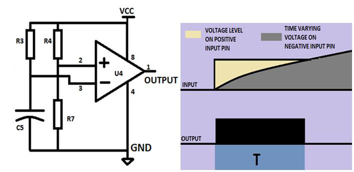
Fig. 24: Circuit Diagram For Mono-Stable Multi-Vibrator And Its Input And Output Waveforms
When it is powered up the circuit simply generates the waveform as shown in the OUTPUT axis of the right hand side plot in the above figure. The output will be high for a particular time period during its quasi-stable state and after that the output become low and continues indefinitely in its stable state.
Now the question is how can we make use of such a circuit in our design to extend the pulses at the output of the comparator? Simply we must get a continuous high output from the above circuit. The only way to do that is never let the capacitor charge up to voltage level of detection. This can be done by periodically discharging the capacitor completely at once before it reaches the voltage level of detection each time. The capacitor will charge itself again and again and once we stop discharging it will charge above the voltage level of detection and the output becomes low.
The capacitor can be discharged by applying a negative or zero volts at the point where the resistor and the capacitor joins together. Our intention is to use the COMPARATOR block’s output with the mono-stable multi-vibrator and the since it has regular period of zero voltages we can use this waveform to discharge the capacitor periodically.
Since we must discharge the capacitor at the rising edge of the pulses so that it won’t charge up to the voltage level of detection whenever a new pulse arrive we must first invert the waveform at the output of the COMPARATOR block before applying it to our circuit.
The waveforms in the following figure will make it more clearly for you.
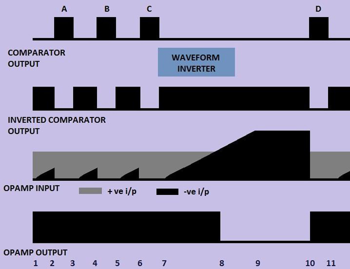
Fig. 25: Comparator Block’s Output Waveform With Mono-Stable Multi-Vibrator
Multivibrator Designing Contdd
The comparator output waveform and its inverted version are plotted in the above timing diagram. The voltages appears on the two inputs of the op-amp are also shown along with the output waveform of the op-amp.
The different significant points in time marked in the above timing diagram is mentioned in detail in the following table:
|
1 |
There is no pulse generated at the comparator output and hence the comparator output is low and it will remain low until the pulse A is generated at 2. The inverted comparator output is high and it will remain high until the comparator output become high again at 2. The capacitor has just started charging and hence voltage at the op-amp negative input slowly increases. Since the voltage at the positive input pin of the op-amp is still higher than the voltage at the negative input pin the output of the op-amp is high and remains high until the capacitor charges to a voltage above the voltage set at the positive input pin. |
|
2 |
The pulse A is generated at the comparator output and hence the comparator output is high and it will remain high until the pulse A ends at 3. The inverted comparator output becomes low and it will remain low until the comparator output become low again at 3. The capacitor suddenly discharges to zero volts due to the zero voltage input appear across the capacitor and hence voltage at the op-amp negative input disappears. Since the voltage at the positive input pin of the op-amp is still higher than the voltage at the negative input pin the output of the op-amp is high and remains high until the capacitor charges to a voltage above the voltage set at the positive input pin. |
|
3 |
The pulse A ends at 3 and hence the comparator output is low and it will remain low until the pulse B is generated at 4. The inverted comparator output is high and it will remain high until the comparator output become high again at 4. The capacitor has just started charging and hence voltage at the op-amp negative input slowly increases. Since the voltage at the positive input pin of the op-amp is still higher than the voltage at the negative input pin the output of the op-amp is high and remains high until the capacitor charges to a voltage above the voltage set at the positive input pin. |
|
4 |
The pulse B is generated at the comparator output and hence the comparator output is high and it will remain high until the pulse B ends at 5. The inverted comparator output becomes low and it will remain low until the comparator output become low again at 5. The capacitor suddenly discharges to zero volts due to the zero voltage input appear across the capacitor and hence voltage at the op-amp negative input disappears. Since the voltage at the positive input pin of the op-amp is still higher than the voltage at the negative input pin the output of the op-amp is high and remains high until the capacitor charges to a voltage above the voltage set at the positive input pin. |
|
5 |
The pulse B ends at 5 and hence the comparator output is low and it will remain low until the pulse C is generated at 6. The inverted comparator output is high and it will remain high until the comparator output become high again at 6. The capacitor has just started charging and hence voltage at the op-amp negative input slowly increases. Since the voltage at the positive input pin of the op-amp is still higher than the voltage at the negative input pin the output of the op-amp is high and remains high until the capacitor charges to a voltage above the voltage set at the positive input pin. |
|
6 |
The pulse C is generated at the comparator output and hence the comparator output is high and it will remain high until the pulse C ends at 7. The inverted comparator output becomes low and it will remain low until the comparator output become low again at 7. The capacitor suddenly discharges to zero volts due to the zero voltage input appear across the capacitor and hence voltage at the op-amp negative input disappears. Since the voltage at the positive input pin of the op-amp is still higher than the voltage at the negative input pin the output of the op-amp is high and remains high until the capacitor charges to a voltage above the voltage set at the positive input pin. |
|
7 |
The pulse C ends at 7 and hence the comparator output is low and it will remain low until the pulse D is generated at 10. The inverted comparator output is high and it will remain high until the comparator output become high again at 10. The capacitor has just started charging and hence voltage at the op-amp negative input slowly increases. Since the voltage at the positive input pin of the op-amp is still higher than the voltage at the negative input pin the output of the op-amp is high and remains high until the capacitor charges to a voltage above the voltage set at the positive input pin. |
|
8 |
No pulse has occurred since the pulse C ended at 7 and hence the inverted comparator output remains high. The charging of the capacitor is uninterrupted due to the absence of zero voltage input across it. At 8, the voltage across the capacitor increases slightly above the voltage level to be detected. Since the voltage at the negative input pin of the op-amp becomes higher than the voltage at the positive input pin the op-amp output suddenly falls to zero for the first time. The op-amp output will remain zero until the voltage at the negative input pin becomes lower than the voltage at the positive input pin. The capacitor continues charging until it reaches the supply voltage at 9 and continues at that voltage thereafter. |
|
9 |
No pulse has occurred since the pulse C ended at 7 and hence the inverted comparator output remains high. The charging of the capacitor is uninterrupted due to the absence of zero voltage input across it. The capacitor continues its charging and the voltage across the capacitor become equal to the supply voltage at 9. From 9 onwards the capacitor remains at the same voltage itself and so does the voltage at the negative input pin of the op-amp. Since the voltage at the negative input pin of the op-amp remains higher than the voltage at the positive input pin the op-amp output remains low. The op-amp output will remain zero until the voltage at the negative input pin becomes lower than the voltage at the positive input pin. |
|
10 |
The pulse D suddenly appears at the comparator output and hence the comparator output is becomes high and it will remain high until the pulse D ends at 11. The inverted comparator output becomes low and it will remain low until the comparator output become low again at 11. The capacitor suddenly discharges to zero volts due to the zero voltage input appear across the capacitor and hence voltage at the op-amp negative input disappears. Since the voltage at the positive input pin of the op-amp becomes higher than the voltage at the negative input pin the output of the op-amp becomes high again and remains high until the capacitor charges to a voltage above the voltage set at the positive input pin. |
|
11 |
The pulse D ends at 11 and hence the comparator output is low and it will remain low until the pulse the next pulse is generated. The inverted comparator output is high and it will remain high until the comparator output become high again. The capacitor has just started charging and hence voltage at the op-amp negative input pin slowly increases. Since the voltage at the positive input pin of the op-amp is still higher than the voltage at the negative input pin, the output of the op-amp is high and remains high until the capacitor charges to a voltage above the voltage set at the positive input pin. |
Fig. 26: Details Of The Timing Diagram For The Mono-Stable With Inverted Waveform Input
We will do the waveform inversion process when we do the design of the complete circuit diagram. We kept that out of the function of this particular block. All we are going to do further in this block is to do a provision to fed the inverted comparator waveform to the input of the circuit and hence across the charging capacitor. The circuit should respond to a zero input voltage only and no response to a positive input voltage. This can be achieved by using a simple diode at the point where the capacitor and the resistor joins together. The commonly used diode PN junction diode 1N4007 can be used for this purpose. Such an arrangement is shown in the following circuit diagram.
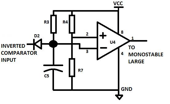
Fig. 27: Circuit Diagram of Monostable Small Block
The completed circuit diagram for the MONOSTABLE SMALL block has been designed and the values of the components are given in the following table:
|
Serial no. |
COMPONENT |
TYPE |
VALUE |
|
1 |
R3 |
resistor |
270 KE |
|
2 |
R4 |
resistor |
1 KE |
|
3 |
R7 |
resistor |
1 KE |
|
4 |
C5 |
Capacitor |
1 mfd |
|
5 |
D2 |
Diode |
1N4007 |
|
6 |
U4 |
Op-amp |
½ LM358 |
Fig. 28: MONOSTABLE SMALL Circuit Component Value
We have done with the MONOSTABLE SMALL circuit design and now let us design a circuit for the MONOSTABLE LARGE block.
MONOSTABLE LARGE:
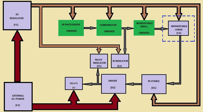
Fig. 29: Block Diagram of Monostable Large Block
We are expecting the MONOSTABLE LARGE block to be a mono-stable circuit with a comparatively high quasi-stable time period. The working of the MONOSTABLE LARGE multi-vibrator is exactly similar to that of the MONOSTABLE SMALL. For the design of the circuit for the MONOSTABLE LARGE block a timely increasing voltage source is generated using an R-C network. The voltage level to be detected is generated using a potential divider network.
The timely increasing voltage is applied to the negative input pin of an op-amp and the voltage level from the potential divider is applied to the positive input pin of the op-amp.
The R-C network and the potential divider network are shown below.
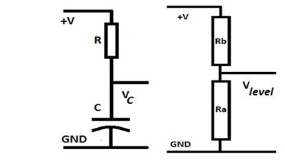
Fig. 30: Circuit Diagram Of R-C Network And Potential Divider Network
The R-C network shown in the above figure is made up of a resistor ‘R’ and a capacitor ‘C’ and the circuit is applied across a voltage ‘V’ and the output voltage ‘Vc’ is taken across the capacitor and the ground.
Suppose if the time taken for the circuit to generate an output voltage ‘Vc’ is ‘T’, then we have the Equation: 6 which relates the input voltage ‘V’, resistance ‘R’, capacitance ‘C’, time period ‘T’ and the final output voltage ‘Vc’.
Vc = V (1-e-T/RC) (Equation: 6)
Where; The product RC is called the time constant of the R-C circuit. Simply this is the factor with which the input voltage is delayed to be completely reflected at the output. Now suppose we need only half of the input voltage at the output, ie. Vc = V/2. Then we have the Equation: 7 give the time taken for the output to reach the half of the inpu
T = 0.693RC (Equation: 7)
In a potential divider network with two resistors ‘Ra’ and ‘Rb’ connected across a voltage ‘V’ and the output voltage ‘Vlevel’ is taken from the point where the ‘Ra’ and ‘Rb’ join together is already given by the Equation: 5
Vlevel = V * (Ra / (Ra + Rb)) (Equation: 5)
Where;
(Ra / (Ra + Rb)) is the factor by which the input voltage ‘V’ is divided
In contrast to the MONOSTABLE SMALL circuit, let us apply the voltage level from the potentials divider to the negative input pin of an op-amp and the voltage across the capacitor to the positive input pin of the op-amp. The output from the MONOSTABLE SMALL block is applied across the capacitor through a diode. Such a circuit is shown in the following diagram.
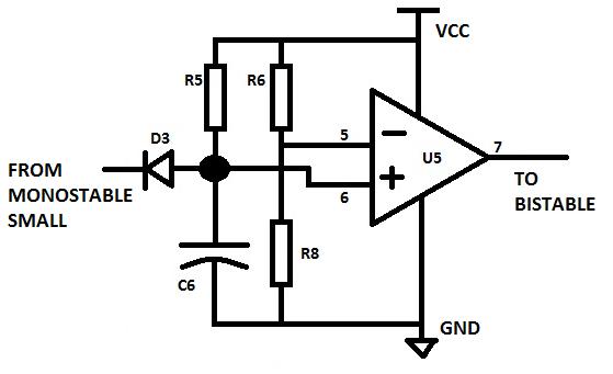
Fig. 31: Circuit Diagram Of Mono-Stable Large
In the above shown circuit the resistors R6 and R8 forms the potential divider network and the resistor R5 together with the capacitor C6 forms the R-C network. The ‘U5’ is the op-amp and the negative input is connected to the voltage level set by the potential divider and the positive pin is connected to the timely increasing input from the R-C network so that the output remains low till the capacitor takes it time charging to a voltage above the voltage detection level.
The significance of the components of the above circuit is mentioned in the following table
|
COMPONENT |
FUNCTION |
|
R6 |
The R6 forms a potential divider network with the R8 and the R6 connects the VCC to the potential divider network. The output from the potential divider network is taken from the point where the R6 connects with the R8. Increasing the value of R4 decreases the voltage output from the potential divider network. |
|
R8 |
The R8 forms a potential divider network with the R6 and the R8 connects the GND to the potential divider network. The output from the potential divider network is taken from the point where the R8 connects with the R6. Increasing the value of R8 increases the voltage output from the potential divider network. |
|
R5 |
The R5 is used along with C6 as an R-C network or a tank circuit. It is through the R5 that the capacitor charges to the input voltage. Increasing the value of the R5 makes the charging process slower and decreasing the value of the R5 makes the charging process faster. |
|
C6 |
The C6 is used along with R5 as an R-C network or a tank circuit. The capacitor C6 charges to the input voltage through the resistor R5. Increase the value of C6 and the capacitor will take more time to charge up to a particular voltage. Hence increasing the value of the C6 makes the charging process slower and decreasing the value of the C6 makes the charging process faster. |
|
U5 |
The U5 is the op-amp used to detect whenever the voltage across the capacitor rises across a predefined value set by the potential divider network. The positive input of the op-amp is connected to the potential divider network and the negative input pin is connected to the output of the R-C network. Whenever the voltage across the capacitor is above the predefined voltage level the output becomes low, otherwise remains high |
|
D3 |
It couples the output from the MONOSTABLE SMALL block and applies it across the charging capacitor C6. The zero voltage is coupled only and prevents the positive voltages from affecting the charging of the circuit |
Fig. 32: Component Significance Of The MONOSTABLE LARGE Circuit
The waveform corresponding to the working of the circuit is shown in the following timing diagram.
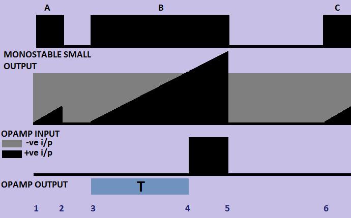
Fig. 33: Timing Diagram Of Monostable Large Circuit
The significant points in time marked in the above timing diagram is mentioned in detail in the following table
|
1 |
The output at the MONOSTABLE SMALL is high due to A and remains high until the A falls at 2. The capacitor in the MONOSTABLE LARGE circuit start charging slowly and hence the voltage at the positive input pin slowly increases. Since the voltage at the positive input pin of the op-amp is smaller than the voltage level fixed at the negative input pin the output voltage of the op-amp remains low until the capacitor charges to a voltage above the voltage level at the negative input pin. |
|
2 |
The output at the MONOSTABLE SMALL becomes low and it will remain low till 3. It suddenly discharges the capacitor to zero volts and hence the voltage at the positive input pin becomes zero. Since the voltage at the positive input pin of the op-amp is smaller than the voltage level fixed at the negative input pin the output voltage of the op-amp remains low until the capacitor charges to a voltage above the voltage level at the negative input pin. |
|
3 |
The output at the MONOSTABLE SMALL becomes high due to B and remains high until the B falls at 5. The capacitor in the MONOSTABLE LARGE circuit starts charging slowly and hence the voltage at the positive input pin slowly increases. Since the voltage at the positive input pin of the op-amp is smaller than the voltage level fixed at the negative input pin the output voltage of the op-amp remains low until the capacitor charges to a voltage above the voltage level at the negative input pin. |
|
4 |
At this point the voltage across the capacitor increases above the voltage level set at the negative input pin. Thus the positive input pin becomes more positive than the negative input pin and the op-amp produces a positive output. The capacitor continue its charging towards the supply voltage and the output of the op-amp remains high until the voltage across the capacitor is larger than the voltage at the negative input pin. The time taken for the output of the op-amp to become high after the input of this circuit starts keeping high is marked as ‘T’ in the timing diagram. ‘T’ is called the quasi-stable state time period of the circuit. |
|
5 |
The output at the MONOSTABLE SMALL becomes low and it will remain low till 6. It suddenly discharges the capacitor to zero volts and hence the voltage at the positive input pin becomes zero. Since the voltage at the positive input pin of the op-amp is smaller than the voltage level fixed at the negative input pin, the output voltage of the op-amp suddenly becomes low and remains low until the capacitor charges to a voltage above the voltage level at the negative input pin. |
|
6 |
The output at the MONOSTABLE SMALL is high due to C and remains high until the C falls. The capacitor in the MONOSTABLE LARGE circuit start charging slowly and hence the voltage at the positive input pin slowly increases. Since the voltage at the positive input pin of the op-amp is smaller than the voltage level fixed at the negative input pin the output voltage of the op-amp remains low until the capacitor charges to a voltage above the voltage level at the negative input pin. |
Fig. 34: Details Of The Timing Diagram For MONOSTABLE LARGE Circuit
Let us select the op-amp as LM358 itself for the MONOSTABLE LARGE circuit also. Now if we set the voltage level at the positive input pin as half the supply voltage we can use the Equation: 7 for calculating the quasi-stable time period ‘T’. The only way to set the voltage detection level as half of the supply voltage is by using the resistors with same value for both the R6 and R8. Hence let us assume the value 1K for both the resistors R6 and R8.
Now let us design the value for R3 and C5. The time period ‘T’ in our actual implementation is the ‘Tex’ the extended time period for the COMPARATOR SMALL and we have already mentioned the value for ‘Tex’ as 15 seconds. Since the voltage level to be detected is half the supply voltage then with the help of the Equation: 7 we can design the values for the resistor R5 and capacitor C6.
From Equation: 7, the time period required to reach the charging capacitor output to reach half the supply voltage in a serial R-C circuit is
T = 0.693RC
We take T = 15 and the value of R5 as 270KE, then
C = 15 / (0.693 * 270000)
And we will get the value for the capacitor around 80 mfd. Let us take the value of the capacitor as standard 100 mfd.
Thus we have done the design for the components for the time period ‘T’ and the value of the components are listed in the following table.
|
COMPONENT |
VALUE |
|
R6 |
1 KE |
|
R8 |
1 KE |
|
R5 |
270 KE |
|
C6 |
100 mfd |
Fig. 35: Component Values Designed For MONOSTABLE LARGE Time Period ‘T’
The completed circuit diagram for the MONOSTABLE LARGE block has been designed and the details of the components are given in the following table:
|
Serial no. |
COMPONENT |
TYPE |
VALUE |
|
1 |
R6 |
resistor |
1 KE |
|
2 |
R8 |
resistor |
1 KE |
|
3 |
R5 |
resistor |
270 KE |
|
4 |
C6 |
Capacitor |
100 mfd |
|
5 |
D3 |
Diode |
1N4007 |
|
6 |
U5 |
Op-amp |
½ LM358 |
Fig. 36: MONOSTABLE LARGE Circuit Component Values
Now there is one more crucial block left to be designed. Let us discuss about the circuit designing of the bi-stable block
Bistable Multivibrator
BI-STABLE BLOCK:
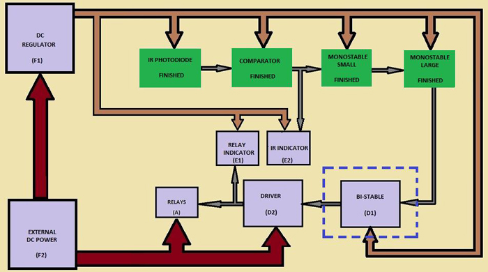
Fig. 37: Block Diagram Of Bi-Stable Circuit
Bi stable is a circuit with two stable states and it can change itself from one state to another on a trigger pulse. There is no quasi-stable state for this bi stable circuit. If there are two states A and B and the output voltage at the state A is say logic high then for state B the output voltage will be logic 0. The states can be toggled by using a trigger pulse. The input trigger pulses and output waveforms are shown in the following figure.

Fig. 38: Input And Output Waveforms For Bi Stable
From the above figure the bi stable was in state A initially and then the pulse 1 triggers the bi stable to state B. It remains in state B until the pulse 2 triggers the bi stable from state B back to state A. The bi stable remains in state A until it is triggered back to state B by pulse 3. Again it remains in state B itself until it is triggered back to state A by pulse 4.
There are various kinds of bi stable circuits available including those using op-amp, but here we are using a totally different kind of circuit. Here the bi stable circuit is realized using a decade counter CD 4017.
CD 4017 is a decade counter IC. It has 10 output pins and only one of them is high at a time. The IC can receive trigger pulses from other circuits and shift the high voltage from one of the output in to the next pin among the 10 output pins. After the 10th pin is high the circuit can be so arranged that the first pin become high again on the next input pulse. Always on of the output pin is high and all others are low.
The CD4017 comes in 16 pin dual inline package and the pin-out of the CD4017 is shown in the following figure.
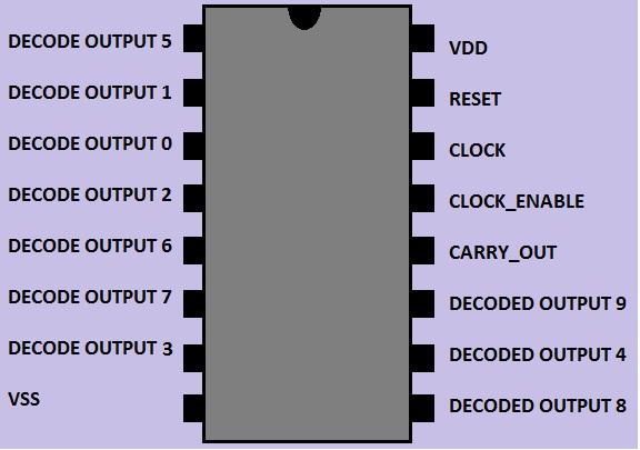
Fig. 39: Diagram of Pin-Out Of CD4017cd4017
The pin description for the cd4017 IC is given in the following table:
|
PIN NUMBER |
PIN |
DESCRIPTION |
|
1 |
DECODE OUTPUT 5 |
This pin becomes high and all other low on the fifth input clock. The pin will remain high till the next pulse arrives. |
|
2 |
DECODE OUTPUT 1 |
This pin becomes high and all other low on the first input clock. The pin will remain high till the next pulse arrives. |
|
3 |
DECODE OUTPUT 0 |
This pin is high initially and all other low. The pin will remain high till the next pulse arrives. |
|
4 |
DECODE OUTPUT 2 |
This pin becomes high and all other low on the second input pulse. The pin will remain high till the next pulse arrives. |
|
5 |
DECODE OUTPUT 6 |
This pin becomes high and all other low on the sixth input pulse. The pin will remain high till the next pulse arrives. |
|
6 |
DECODE OUTPUT 7 |
This pin becomes high and all other low on the seventh input pulse. The pin will remain high till the next pulse arrives. |
|
7 |
DECODE OUTPUT 3 |
This pin becomes high and all other low on the third input pulse. The pin will remain high till the next pulse arrives. |
|
8 |
VSS |
The ground should be applied to this pin. |
|
9 |
DECODE OUTPUT 8 |
This pin becomes high and all other low on the eighth input pulse. The pin will remain high till the next pulse arrives. |
|
10 |
DECODE OUTPUT 4 |
This pin becomes high and all other low on the fourth input pulse. The pin will remain high till the next pulse arrives. |
|
11 |
DECODE OUTPUT 9 |
This pin becomes high and all other low on the ninth input pulse. The pin will remain high till the next pulse arrives. |
|
12 |
CARRY_OUT |
This pin is high initially and it will toggle its state on every fifth input pulse. The pulse generated at this pin can be used as a clock for the successive 4017 IC in such a way that each time the first 4017 finishes a count of ten the CARRY_OUT pin’s low to high transition clocks the next 4017 and advances its count. |
|
13 |
CLOCK_ENABLE |
This pin is active low. The clock applied can advance the count in a 4017 only if this pin is held low. |
|
14 |
CLOCK |
This is the pin where the clock is applied for advancing the count. The CLOCK pin is positive edge triggered, means the count will be incremented on the low to high transition of the voltage applied on the CLOCK pin. |
|
15 |
RESET |
This is the master reset pin. Applying a positive voltage on this pin will completely reset the 4017. |
|
16 |
VDD |
The positive voltage should be applied to this pin |
Fig. 40: CD4017 Pin-out
The above table gives you a brief description of the pins and their functions in the CD4017. Now the question is how we can make use of the CD4017 to act like a bi stable circuit. Consider pin number 3, DECODE OUTPUT 0. It changes its state from high to low on the first clock pulse. Normally it will remain low till the next 9 pulses. Suppose if we use a technique in such a way that the CD4017 will reset on the second clock pulse and since the reset value of the DECODE OUTPUT 0 is high it will become high on that second clock pulse. That means using such a technique the DECODE OUTPUT 0 is logic one initially, on first clock it becomes zero and on second clock pulse it becomes logic one again and this process continues for the following pulses. Thus the DECODE OUTPUT 0 pin acts as a bi stable.
How can we implement such a technique in the CD4017? The answer is simply connecting the next output in the row, which is supposed to become high on the arrival of second clock pulse on to the reset pin of the CD4017; you can take the bi stable output from the DECODE OUTPUT 0. Such an arrangement is shown in the following circuit diagram.
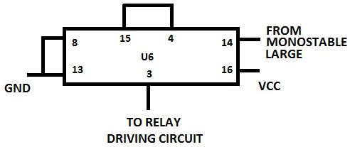
Fig. 41: Circuit Diagram Of CD4017 Relay Driving
As you can see from the above circuit the pin number 4 which is the DECODE OUTPUT 2 is shorted with the pin number 15 which is the RESET pin. Pin number 13 which is the CLOCK_ENABLE pin is also grounded along with the pin number 8 which is the VSS pin so as to enable the clocking.
The working of the above circuit can be easily understood from the following timing diagram. We need to consider the voltages on these pins; CLOCK, DECODE OUTPUT 0, DECODE OUTPUT 1, DECODE OUTPUT 2 and RESET. Keep in mind that we have the CLOCK pulses from the previous MONOSTABLE LARGE block and we are taking the bi stable output from the pin DECODE OUTPUT 0.

Fig. 42: Timing Diagram Of Bi Stable CD4017
The waveforms at different pins are plotted in the above timing diagram and the details of the important points marked are mentioned in the following table.
|
1 |
The CD4017 was in the reset state and hence the DECODE OUTPUT 0 pin was high and DECODE OUTPUT 1 and DECODE OUTPUT 2 pins were low. RESET pin was also low. At ‘1’ the pulse A appears at the CLOCK pin and rising edge of the pulse A advances the counter one step. The DECODE OUTPUT 1 becomes high, DECODE OUTPUT 0 becomes low, DECODE OUTPUT 2 and RESET pin remains low till the rising edge of the pulse B arrives at 3. |
|
2 |
The pulse A ends here and the falling edge of the pulse has no effect on the output. The DECODE OUTPUT 1 remains high; DECODE OUTPUT 0, DECODE OUTPUT 2 and RESET pin remains low till the rising edge of the pulse B arrives at 3. |
|
3 |
At this point pulse B appears at the CLOCK pin and rising edge of the pulse B advances the counter one step. The DECODE OUTPUT 1 becomes low. Normally the DECODE OUTPUT 2 should become high and remains high, since the DECODE OUTPUT pin is connected to the RESET pin; a logic high voltage on this pin suddenly resets the entire circuit. Hence the DECODE OUTPUT 2 remains high for a very small period of time only and by that time the device resets and DECODE OUTPUT 0 becomes high again and DECODE OUTPUT 1 becomes low. |
|
4 |
The pulse B ends here and the falling edge of the pulse have no effect on the output. The DECODE OUTPUT 1, DECODE OUTPUT 2 and RESET pin remains low and DECODE OUTPUT 0 remains high till the rising edge of the pulse C arrives at 5. |
|
5 |
The pulse C appears at the CLOCK pin and rising edge of the pulse C advances the counter one step. The DECODE OUTPUT 1 becomes high, DECODE OUTPUT 0 becomes low, DECODE OUTPUT 2 and RESET pin remains low till the rising edge of the pulse D arrives at 7. |
|
6 |
The pulse C ends here and the falling edge of the pulse have no effect on the output. The DECODE OUTPUT 1 remains high; DECODE OUTPUT 0, DECODE OUTPUT 2 and RESET pin remains low till the rising edge of the pulse D arrives at 7. |
|
7 |
At this point pulse D appears at the CLOCK pin and rising edge of the pulse D advances the counter one step. The DECODE OUTPUT 1 becomes low. Normally the DECODE OUTPUT 2 should become high and remains high, since the DECODE OUTPUT pin is connected to the RESET pin; a logic high voltage on this pin suddenly resets the entire circuit. Hence the DECODE OUTPUT 2 remains high for a very small period of time only and by that time the device resets and DECODE OUTPUT 0 becomes high again and DECODE OUTPUT 1 becomes low. |
|
8 |
The pulse D ends here and the falling edge of the pulse have no effect on the output. The DECODE OUTPUT 1, DECODE OUTPUT 2 and RESET pin remains low and DECODE OUTPUT 0 remains high till the rising edge of the pulse E arrives at 9. |
|
9 |
The pulse D appears at the CLOCK pin and rising edge of the pulse D advances the counter one step. The DECODE OUTPUT 1 becomes high, DECODE OUTPUT 0 becomes low, and DECODE OUTPUT 2 and RESET pin remains low till the rising edge of the next pulse arrives. |
|
10 |
The pulse D ends here and the falling edge of the pulse have no effect on the output. The DECODE OUTPUT 1 remains high; DECODE OUTPUT 0, DECODE OUTPUT 2 and RESET pin remains low till the rising edge of the next arrives. |
Fig. 43: CD4017 Bi Stable Circuit Timing Diagram Details
The above timing diagram and the details given in the table might have given you a complete idea about this particular bi stable circuit. The details of the components of this bi stable circuit are given in the following table
|
Serial no. |
COMPONENT |
TYPE |
VALUE |
|
1 |
U6 |
DECADE COUNTER |
CD4017 |
Fig. 44: Component Details Of BISTABLE Block Circuit
We haven’t finished designing the circuit for the functional blocks, still few more blocks left. But with the BISTABLE block we can say that we have done the circuit design for all the crucial functional blocks. Let us finish the other functional blocks also and consider the DRIVER block next.
DRIVER BLOCK:
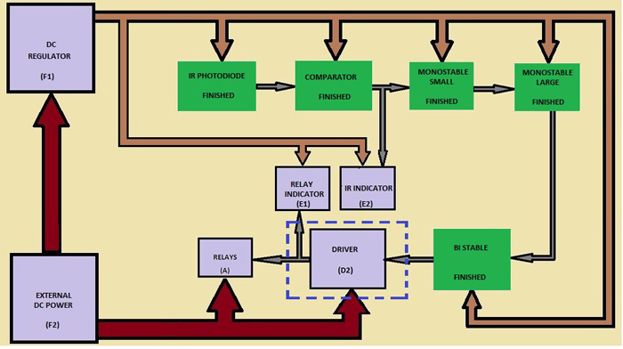
Fig. 45: Block Diagram Of Driver
We are using the DRIVER block to drive the RELAYS since the output from the BISTABLE block can’t source enough power at that voltage to drive the relays. The drivers are simply power amplifiers. Power amplifier usually amplifies the current keeping the voltage constant or amplifies both the current and voltage since the power is the product of voltage and current.
P = VI (Equation: 8)
Where;
P is the power input to a load
V is the voltage across the load
I is the current flowing through the load
In our case the relays just won’t work in the 5V regulated supply and also the current is very small, so we need to amplify both the current and the voltage.
When we talk about the amplifiers, the first thing that comes to our mind is transistor. Here also there is no exception, we are going to design a power amplifier using a transistor.
How much current we need to drive the RELAYS block? I think 1 ampere will be good enough. Let us start the design for the following transistor based current amplifier circuit.
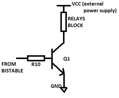
Fig. 46: Circuit Diagram Of Transistor Based Current Amplifier
The above shown circuit is called Class B power amplifier. The RELAYS block as such is introduced as the load for the amplifier. The entire current flows through the transistor will flow through the load also. In this case we actually don’t have the usual kind of signals that we use with the Class B amplifier. We have a DC signal that is sometimes logic zero (~0 volt) and sometimes logic one (~5 volt). Thus we have an ON-OFF signal input for this amplifier and the transistor amplifier function is reduced to ON and OFF the RELAY block only. Keeping this in mind our intention is just to design the right value for the resistor R10 so as to set the current during the transistor is ON to approximately 1 ampere.
The curren flowing through the RELAY block is actually the collector current of the transistor and there is a relation between the collector current and the base current of the transistor as given in the following equation.
Ic =hfe * Ib (Equation: 9)
Where;
‘Ic’ is the collector current of the transistor
‘Ib’ is the base current of the transistor and
‘hfe’ is called the current gain of the transistor. It is actually the factor by which the base current is amplified to get the collector current
Let us represent the base current as ‘Ib’ and collector current as ‘Ic’ and voltage across the base and emitter as ‘Vbe’ and the voltage equivalent to the logic 1 input as Vin in the circuit as shown below.
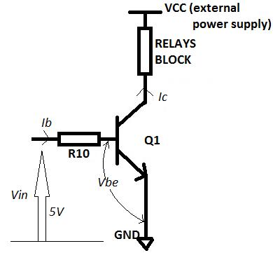
Fig. 47: Circuit Diagram Of Driver
Let us use the NPN general purpose transistor SL100 for the above design. The SL100 has a maximum Vbe of 1.3 volts and maximum hfe of 300. These values depend on the operation voltages. Hence let us assume an approximate value 100 for hfe and 1 volt for Vbe.
We have,
Vin = 5V and Vbe = 1 V,
Then the voltage across the resistor R10 is Vin~Vbe = 4 V.
We need Ic = 1 ampere and we have hfe = 100, hence from the Equation: 9
Ic =hfe * Ib (Equation: 9)
The Ib can be calculated as
Ib = Ic/hfe = 1/100 amperes = 0.01 amperes
Now we have the current flowing through the resistor R10 which is ‘Ib’ = 0.01 amperes and
The voltage across the resistor = 4 volts
Using the Equation: 4
V = IR (Equation: 4)
The resistance can be calculated as V/I and here the V = 4 volts and I = 0.01 amperes. Hence
R10 = 4/0.01 = 400 ohms.
Let us take the 550 ohm standard resistor value for the R10.
Thus we have designed the values for the components of the DRIVER circuit based on the Class B transistor configuration and the details of the components of this bi stable circuit are given in the following table
|
Serial no. |
COMPONENT |
TYPE |
VALUE |
|
1 |
Q1 |
NPN TRANSISTOR |
SL100 |
|
2 |
R10 |
RESISTOR |
550 E |
Fig. 48: Driver Circuit Component Details
The functions of the components used in the circuit diagram of the DRIVER block are mentioned in the following table
|
COMPONENT |
FUNCTION |
|
R10 |
This is the base resistor and is used to set the collector current of the transistor in a required range by controlling the current flowing to the base when a logic high input is applied. Increasing the value of the base resistor decreases the current flowing towards the base and hence decreases the collector current of the transistor. Decreasing the value of the base resistor increases the current flowing towards the base and hence increases the collector current of the transistor |
|
Q1 |
This transistor is used as a power amplifier and is connected in a Class-B power amplifier configuration. It generate an output collector current which is the product of the base current and the current gain of the transistor |
Fig. 49: Functions Of The Components In DRIVER Circuit
From the complete block diagram we can see that the DRIVER block is also connected to the RELAY INDICATOR block. Let us take the output for the RELAY INDICATOR block from the collector of the transistor itself as shown in the following circuit.
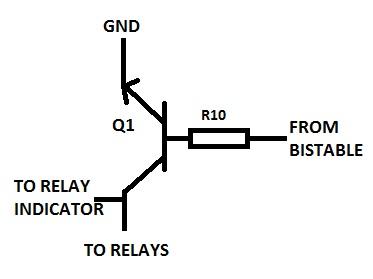
Fig. 50: Circuit Diagram of Input And Output of Driver
Whenever the transistor is ON the voltage output for the RELAY INDICATOR will be low and whenever the transistor is OFF the voltage output for the RELAY INDICATOR will be high. With that we’ve finished the design for the DRIVER module and now let us start the design for the indicator modules.
RELAY INDICATOR:
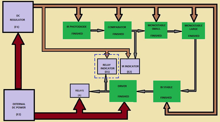
Fig. 51: Block Diagram Of Relay-Indicator
We better use two LEDs to represent the states of the relays. When there is zero voltage appears for the RELAYS block a GREEN LED glows and when there is a high voltage appears at the input of the RELAYS block a RED LED glows. Such an arrangement can be done with LEDs and current limiting resistors as shown in the following circuit.
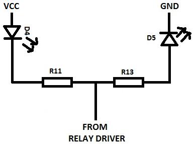
Fig. 52: Circuit Diagram Of Relay-Indicator
The functions of the components used in the above circuit is mentioned in the following table
|
COMPONENT |
FUNCTION |
|
D4 |
The D4 glows when the output from the DRIVER block is logic zero voltage. |
|
R11 |
This is the current limiting resistor for the D4 LED and it controls the current flowing through the LED when it is ON. Increasing the value of the resistor will decrease the current flowing through the D4 LED and hence reduces its brightness and decreasing the value of resistance will increase the current flow and hence increases the brightness. |
|
D5 |
The D5 glows when the output from the DRIVER block is logic high voltage. |
|
R13 |
This is the current limiting resistor for the D5 LED and it controls the current flowing through the LED when it is ON. Increasing the value of the resistor will decrease the current flowing through the D4 LED and hence reduces its brightness and decreasing the value of resistance will increase the current flow and hence increases the brightness. |
Fig. 53: Functions Of The Components In Circuit Of RELAY INDICATOR Block
The working of the above circuit can be explained as follows. When the voltage from the DRIVER block is zero the LED marked as D4 will be forward biased through the resistor R11 and the LED marked as D5 will be reverse biased through the resistor R13. Hence the D4 LED glows and the D5 LED remains OFF. When the voltage from the DRIVER block is logic high, the LED marked as D4 will be reverse biased through the resistor R11 and the LED marked as D5 will be forward biased through the resistor R13. Hence the D5 LED glows and the D4 LED becomes OFF.
The R11 and R13 resistors are used as current limiting resistors for limiting the current flowing through the LEDs when they forward biases. Let us assume their values as 1K each.
Thus we have designed the circuit for the RELAY INDICATOR block and the details of the components of the circuit are given in the following table
|
Serial no. |
COMPONENT |
TYPE |
VALUE |
|
1 |
R11 |
RESISTOR |
1 KE |
|
2 |
R13 |
RESISTOR |
1 KE |
|
3 |
D4 |
LED |
RED |
|
4 |
D5 |
LED |
YELLOW |
Fig. 54: Component Details Of The RELAY INDICATOR Block
IR INDICATOR:
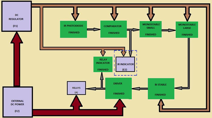
Fig. 55: Block Diagram Of IR-Indicator
This block is used as an indication of the IR pulses received by the device from the TV remote and we are taking the input for this block from the COMPARARTOR block. We are using a LED in series with a resistor for this bock also. The circuit is shown in the following figure
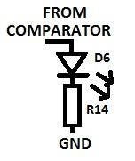
Fig. 56: Circuit Diagram Of IR-Indicator
The functions of the components used in the above circuit is mentioned in the following table
|
COMPONENT |
FUNCTION |
|
D6 |
The D6 glows when the output from the COMPARATOR block is logic high voltage. |
|
R14 |
This is the current limiting resistor for the D6 LED and it controls the current flowing through the LED when it is ON. Increasing the value of the resistor will decrease the current flowing through the D6 LED and hence reduces its brightness and decreasing the value of resistance will increase the current flow and hence increases the brightness. |
Fig. 57: Functions Of The Components In Circuit Of RELAY INDICATOR Block
The R14 is a current limiting resistor and can be used to limit the current flowing through the LED D6. We can use a resistor with 1 KE for the current limiting purpose.
This was the simplest design we have done in this entire project and the values of the components are shown in the following table:
|
Serial no. |
COMPONENT |
TYPE |
VALUE |
|
1 |
D6 |
LED |
RED |
|
2 |
R14 |
RESISTOR |
1 KE |
Fig. 58: Component Details Of The IR INDICATOR Block
Now there we are going to design the regulated power supply block and we have mentioned it as the DC REGULATOR in the complete block diagram.
DC Regulator
DC REGULATOR:
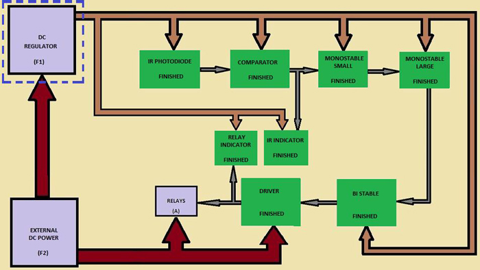
Fig. 59: Block Diagram Of DC Regulator
As we have already mentioned that a power supply regulator is a device which works on DC voltages and it can maintain its output precisely at a fixed voltage always even if there is significant variation in the input DC voltage.
To maintain a precise voltage we normally use regulator ICs in the circuit following the power supply input. A regulator IC is commonly used with capacitors in parallel with the input and output of the regulator IC. We use filter capacitors which are capacitors with comparatively large value for the purpose of checking large variations in the input and output voltages. For very short duration spikes appearing on the input and output we are using bypass capacitors for checking them. Bypass capacitors are very small valued capacitors for bypassing the very short duration pulses directly to the ground.
A circuit with the regulator IC and the above mentioned arrangements is shown in the following figure.

Fig. 60: Circuit Diagram Of Regulated Power Supply
The functions of the components used in the above circuit is mentioned in the following table:
|
COMPONENT |
FUNCTION |
|
C1 |
This capacitor is called bypass capacitor and is used to bypass very short duration spikes to the ground without affecting the other components. |
|
C2 |
This is the filter capacitor used to stabilize the slow variations in the input voltage to the circuit. Increasing the value of the capacitor increase the stabilization and decreasing the value of the capacitor decreases the stabilization. However this capacitor is not good enough to check very narrow duration spikes appears at the input. |
|
C3 |
This is the filter capacitor used to stabilize the slow variations in the output voltage from the circuit. Increasing the value of the capacitor increase the stabilization and decreasing the value of the capacitor decreases the stabilization. However this capacitor is not good enough to check very narrow duration spikes occurs at the output. |
|
C4 |
This capacitor is called bypass capacitor and is used to bypass very short duration spikes to the ground without affecting the other components |
|
U1 |
This is the positive DC regulator IC and it can maintain the output voltage constant precisely at a particular value even though there are significant variations in the input voltage. |
Fig. 61: Functions Of The Components In Circuit Of DC REGULATOR Block
Since we have designed the entire circuit so far to be operated on 5 V DC, we must use a 5 V DC regulator IC. The most common regulator IC available for 5 V DC regulation purpose is 7805 and we are using the same IC as U1 in the above circuit diagram.
The 7805 is a 5 V positive DC regulator IC. It is very versatile and is widely used in all kind of circuits as a voltage regulator. It comes in a three pin package with pins namely INPUT, GROUND and OUTPUT. The pin out of the 7805 is shown in the following figure:
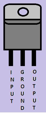
Fig. 62: Diagram Of Pin-Out Of 7805
The pin description of the 7805 is given in the following table:
|
PIN NUMBER |
PIN |
DESCRIPTION |
|
1 |
INPUT |
This is the pin where the positive unregulated voltage is applied for regulation. |
|
2 |
GROUND |
This is the pin where the ground is applied. This pin is common for both the input and output. |
|
3 |
OUTPUT |
When input positive voltage and ground is applied the 5 volt positive regulated voltage will be available at this pin. |
Fig. 63: 7805 IC Pin Description
The capacitors C2 and C3 are filter capacitors and the C1 and C4 are the bypass capacitors in the circuit diagram. The polarized electrolyte capacitors are used for this purpose. We normally use values of 100mfd or more for the filter capacitors. We can use a capacitor of value 1000 mfd for this project. The bypass capacitors are always 0.1 mfd is all kind of circuits. Normally un-polarized capacitors especially disc capacitors are used for this purpose.
Now we have the circuit for the 5 V positive DC regulation and we know the values of the components used as well. The details of the components used in the 5 V positive DC regulator circuit is given in the following table:
|
Serial no. |
COMPONENT |
TYPE |
VALUE |
|
1 |
C1 |
CAPACITOR |
0.1 mfd |
|
2 |
C2 |
CAPACITOR |
1000 mfd |
|
3 |
C3 |
CAPACITOR |
1000 mfd |
|
4 |
C4 |
CAPACITOR |
0.1 mfd |
|
5 |
U1 |
POSITIVE DC REGULATOR |
7805 |
Fig. 64: 7805 Component Details
Now there is only one more functional block left to be designed in the entire block diagram and it is nothing but the RELAYS block itself.
RELAYS:
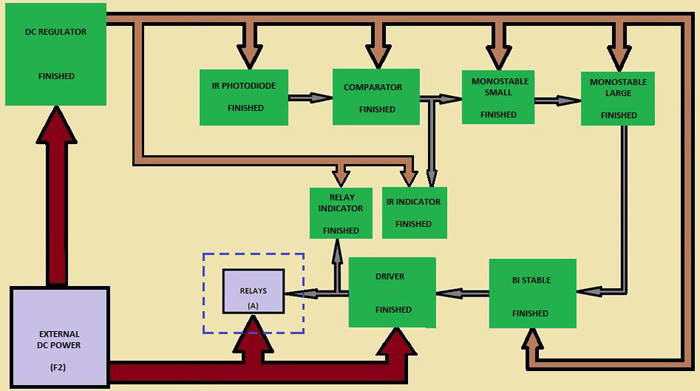
Fig. 65: Block Diagram Of Relays
We are using three SPDT relays to switch the audio video signals from the DVD player and the set top box. We have already mentioned this when we were discussing about the RELAYS block. The three relays can be used as shown in the following figure

Fig. 66: Three SPDT Relays To Switch Audio Video Signals
In our case we need all of them to turn ON or OFF when at the same time. Also it should be noted that there is a single output line running from the DRIVER block. We need to arrange the relays in such a way that the entire relays can be turned ON or OFF using that single line. Such an arrangement of the relays are shown in the following circuit diagram

Fig. 67: Circuit Diagram Of Arrangment of Three Relays
The meaning of the labels that you can see in the above circuit diagram is mentioned in the following table.
|
LABEL |
MEANING |
|
Vdvd |
The video signal output from the DVD player |
|
Vtv |
The video signal input to the TV |
|
Vstpbx |
The video signal output from the DTH set top box |
|
Ldvd |
The audio signal output for the left loudspeaker from the DVD player |
|
Ltv |
The audio signal input for the left loudspeaker to the TV |
|
Lstpbx |
The audio signal output for the left loudspeaker from the DTH set top box |
|
Rdvd |
The audio signal output for the right loudspeaker from the DVD player |
|
Rtv |
The audio signal input for the right loudspeaker to the TV |
|
Rstpbx |
The audio signal output for the right loudspeaker from the DTH set top box |
Fig. 68: RELAYS Circuit Diagram Labels
In the above circuit diagram RL1, RL2 and RL3 are the relays used to switch the signals and D4, D5 and D6 are freewheeling diodes. The freewheeling diodes are normal diodes connected in parallel to the relay coil to prevent back EMF of the coil from affecting other circuits.
Suppose the relay is ON and the current flows through the coil continuously for a considerable amount of time. Due to this current flow a voltage is generated across the coil. When we suddenly turn OFF the relay the current flowing through it is supposed to be vanished instantaneously. This sudden change in current flow can induce a voltage spike with the opposite polarity across the relay coil. This negative polarity spikes can affect the working or can damage the components.
The freewheeling diode is connected in such a way that it becomes forward biased when there is a reverse polarity voltage across the coil. Thus the freewheeling diode simply forms a short circuit path for the reverse polarity signal and hence it does not affect other components.
The functions of the component used in the circuit diagram of the RELAYS block is mentioned in the following table
The functions of the components of the circuit discussed above in listed in the following table
|
COMPONENT |
FUNCTION |
|
RL1 |
The common lead of this relay is connected to the video input of the TV, NO lead is connected to the video output from the DVD player and the NC lead is connected to the video output from the DTH set top box. It is hence used to switch the video signals from the DVD and DTH to the TV. |
|
RL2 |
The common lead of this relay is connected to the left audio input of the TV, NO lead is connected to the left audio output from the DVD player and the NC lead is connected to the left audio output from the DTH set top box. It is hence used to switch the left audio signals from the DVD and DTH to the TV. |
|
RL3 |
The common lead of this relay is connected to the right audio input of the TV, NO lead is connected to the right audio output from the DVD player and the NC lead is connected to the right audio output from the DTH set top box. It is hence used to switch the right audio signals from the DVD and DTH to the TV. |
|
D4 |
This is the freewheeling diode use to prevent the back EMF generated by the RL1 from affecting other circuits. |
|
D6 |
This is the freewheeling diode use to prevent the back EMF generated by the RL2 from affecting other circuits. |
|
D5 |
This is the freewheeling diode use to prevent the back EMF generated by the RL3 from affecting other circuits. |
Fig. 69: The Functions Of The Components Used In RELAY Circuit
We can use the commonly available 1N4007 as the freewheeling diode. Make sure that you’ve connected the diode in such a way that it is reverse biased when you apply voltage to turn ON the relay. I’ve use the sugar cube type 6 V relay for the project.
With this RELAY block we have finished designing circuits for the entire functional blocks shown in the complete circuit diagram. The circuit diagrams of the functional blocks are once again shown below:
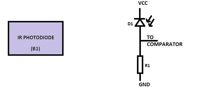
Fig. 70: Block And Circuit Diagram Of IR Photodiode
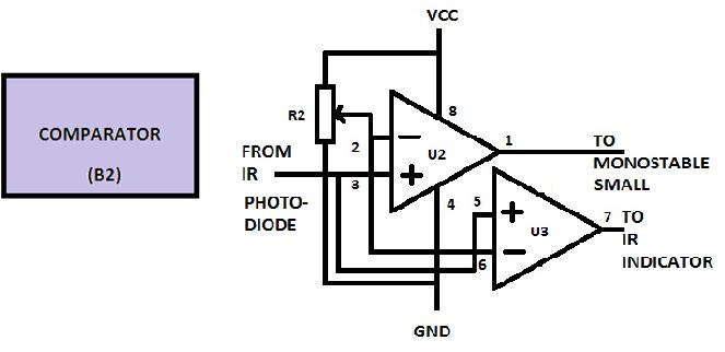
Fig. 71: Block And Circuit Diagram Of Comparator
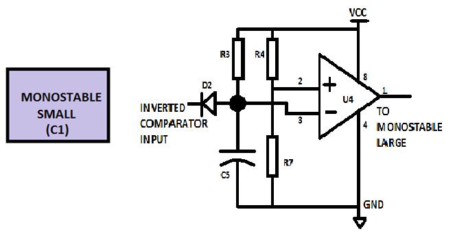
Fig. 72: Block And Circuit Diagram Of Monostable Small
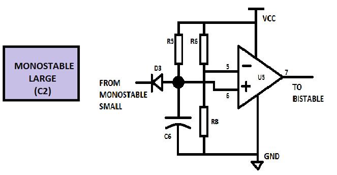
Fig. 73: Block And Circuit Diagram Of Monostable Large
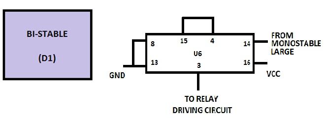
Fig. 74: Block And Circuit Diagram Of Bi Stable
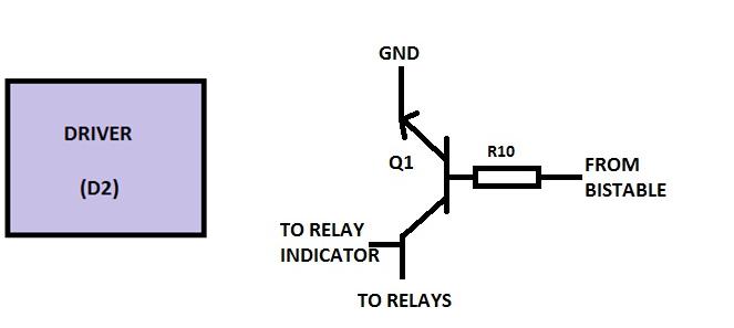
Fig. 75: Block And Circuit Diagram Of Driver

Fig. 76: Block And Circuit Diagram Of Relay Indicator
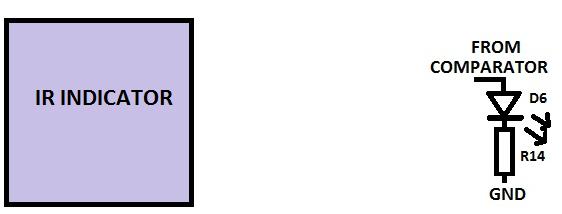
Fig. 77: Block And Circuit Diagram Of IR Indicator

Fig. 78: Block And Circuit Diagram Of DC Regulator
We have the circuit design for all the functional blocks and now it is time to move on to the next step where we will be combining the different circuit design to one single circuit.
Individual circuit diagram to final complete circuit diagram
Step: 6) Individual circuit diagram to final complete circuit diagram
In this step we will combine the individual circuit diagrams into a single circuit diagram for the project. We know how the individual functional blocks are connected in the block diagram and we connect the individual circuit diagrams together referring to those connections.
Let us start with connecting the circuits of IR PHOTODIDOE block with the COMPARATOR block as marked in the following figure.
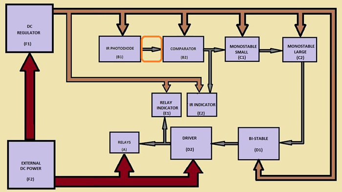
Fig. 79: Block Diagram Of Connecting IR Photodiode and Comparator Circuits
The IR PHOTODIODE circuit can be connected directly to the COMPARATOR circuit without any modification and the connected circuit is shown below.
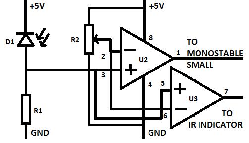
Fig. 80: Circuit Diagram With Connected IR Photodiode and Comparator
Now let us connect the circuit of the COMPARATOR block with the IR INDICATOR block and the MONOSTABLE SMALL block as marked in the following figure
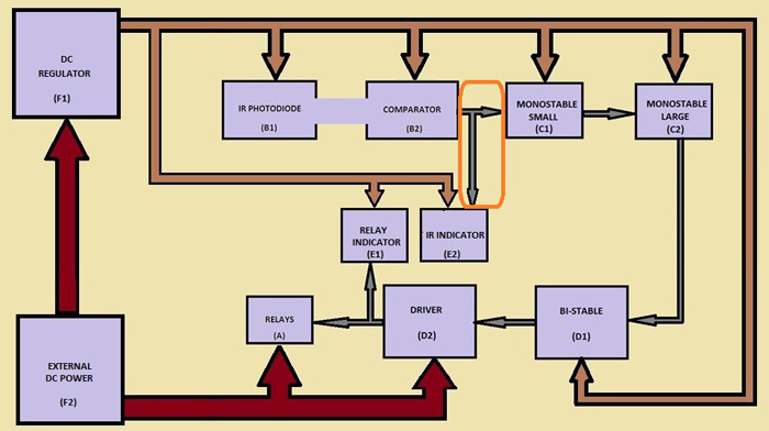
Fig. 81: Block Diagram OF Connecting Comparator With Monostable Small And IR Indicator Circuits
We can connect the IR indicator circuit directly with the COMPARATOR circuit without any modification on both the circuits and the connected circuit is shown below.
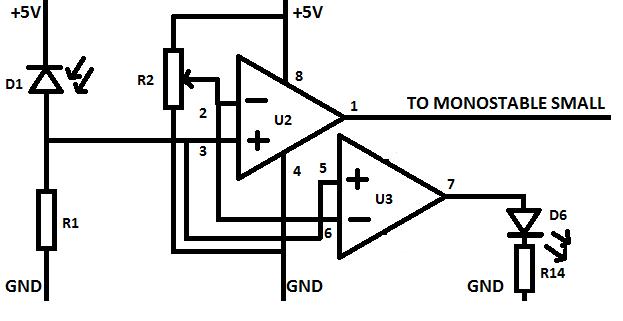
Fig. 82: Circuit Diagram Of Connected IR Indicator With Comparator
But when it comes to connecting the COMPARATOR block with the MONOSTABLE SMALL block we need to do some modifications in the COMPARATOR circuit. The reason is that the MONOSTABLE SMALL block expects an inverted waveform generated by the IR pulses as we have already mentioned in the timing diagram of the MONOSTABLE SMALL circuit which is shown below.
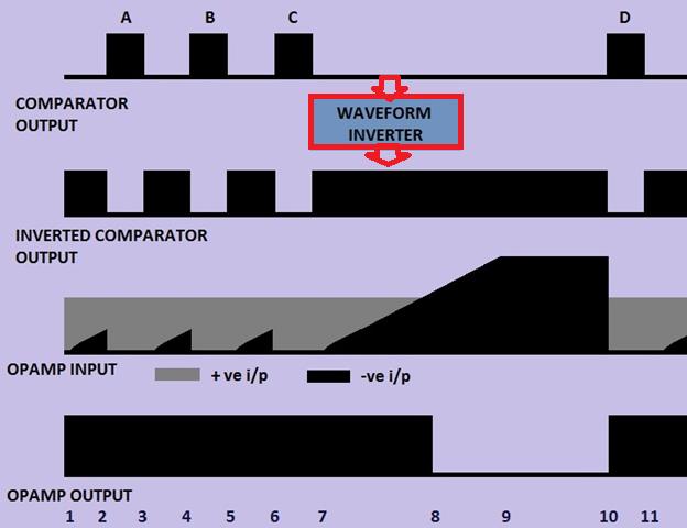
Fig. 83: Waveform Inverter
We don’t need any extra circuit to invert the waveform output of the COMPARATOR to the MONOSTABLE SMALL block rather we will invert the input pins of the comparator U2 and it will do the job for us. The corresponding circuit is shown in the following figure

Fig. 84: Circuit Diagram Of Connected Comparator, IR Indicator and Monostable Small
Now we need to connect the MONOSTABLE SMALL with the MONOSTABLE LARGE circuit as marked in the following figure.
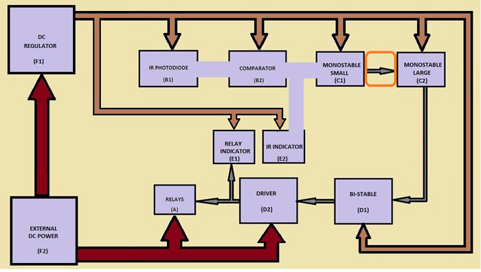
Fig. 85: Block Diagram Of Connected Monostable Small With Monostable Large
The circuit developed so far can be connected with the circuit of the MONOSTABLE LARGE block without any modification required. The connected circuit is shown in the following figure:

Fig. 86: Circuit Diagram Of Connected Monostable Small With Monostable Large
Next we are going to connect the circuit developed so far with the BISTABLE circuit as marked in the following figure.
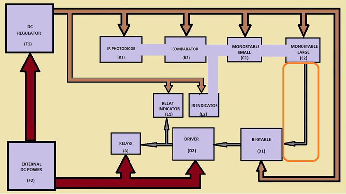
Fig. 87: Block Diagram Of Connected Monostable Large With Bistable Circuit
The bi stable is a positive edge triggered device and it would be better if you connect a pull down resistor with the input of the bi stable. The pull down resistor is used to set the default input voltage to be logic low when there is no device connected at the input of the bi stable circuit. A 1 KE resistor can be used for the purpose of pull down. The circuit connection is as shown in the following figure.
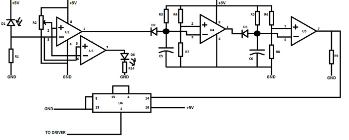
Fig. 88: Circuit Diagram of Connected Monostable Large With Bistable
Next we are going to add the circuit of the DRIVER block with the circuit we have developed so far as marked in the following figure.
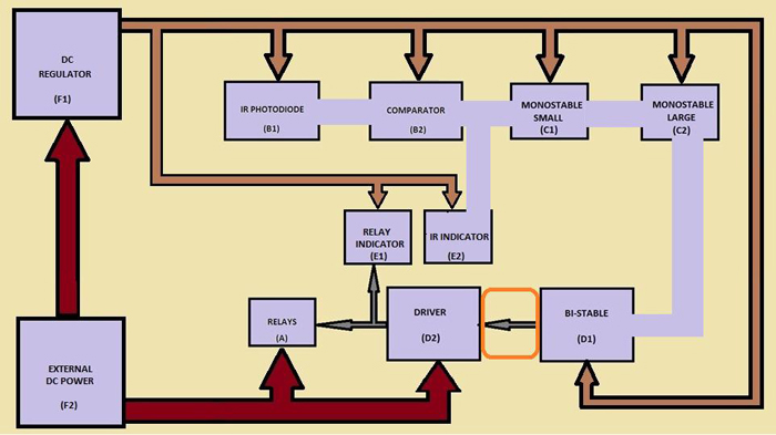
Fig. 89: Block Diagram Of Connected Bistable With Driver Block Circuit
The bi stable circuit can be connected directly with the driver circuit without any modification required and the connected circuit is as shown below.
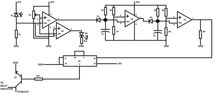
Fig. 90: Circuit Diagram Of Connected Bistable With Driver Block Circuit
Now let us connect the circuit for the RELAYS and the RELAY INDICATOR with the circuit we have developed so far as marked in the following figure.
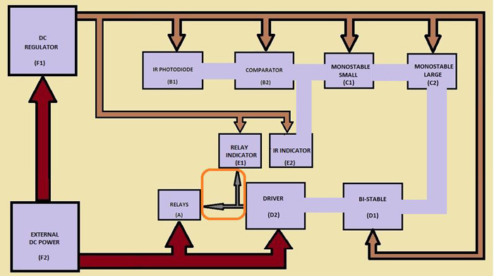
Fig. 91: Block Diagram Of Connected Driver With Relays Block And Relay Indicator Block Circuit
The DRIVER block can be connected directly with the RELAYS and the RELAY INDICATOR block without any problem. But it would be better to add a pull up resistor at the input of the RELAY INDICATOR block so as to set a default positive voltage as input whenever there is no device connected with the indicator circuit. We can use a 1 KE resistor for the pull up purpose. The circuit which is arranged in such a way is shown in the following figure.
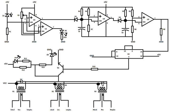
Fig. 92: Circuit Diagram Of Connected Driver, Relays And Relay Indicator Circuits
Now it is time to connect the regulated DC to the circuit wherever it is required as shown in the following figure.
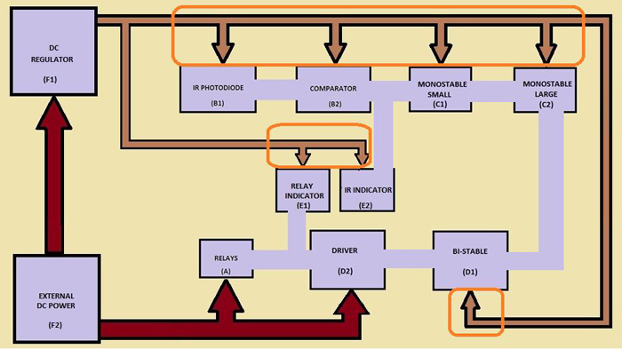
Fig. 93: Block Diagram Of Connecting DC Regulator Circuit With All Other Circuits
Connect all the ‘+5V’ marks to the positive output of the DC REGULATOR circuit and ‘GND’ marks to the ground of the DC REGULATOR circuit. The circuit with the DC regulator supply is shown in the following figure.
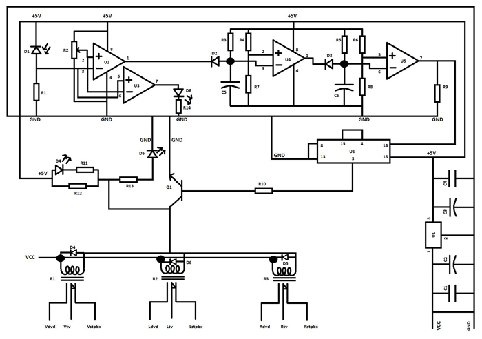
Fig. 94: Circuit Diagram Of Connecting DC Regulator Circuit With All Other Circuits
Now all we need is to connect the external power supply lines to the RELAYS, DRIVER and the DC REGULATOR circuits as marked in the following figure.
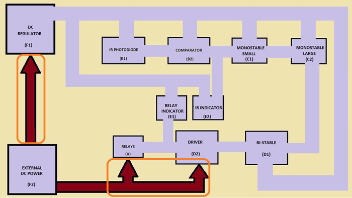
Fig. 95: Block Diagram Of Connecting External DC Power With Relays Driver And DC Regulator
The DC REGULATOR circuit and the RELAYS circuit can be connected directly with the corresponding positive and ground lines of the external power supply. The ground is connected to the ground of the DC REGULATOR circuit, the positive to the positive of DC REGULATOR and the RELAYS. There is no need to actually connect the positive of the EXTERNAL DC POWER with the DRIVER circuit since it will get the positive voltage through the relay coils which is connected in series with the DRIVER circuit. The final circuit diagram with all the connections done is shown in the following figure
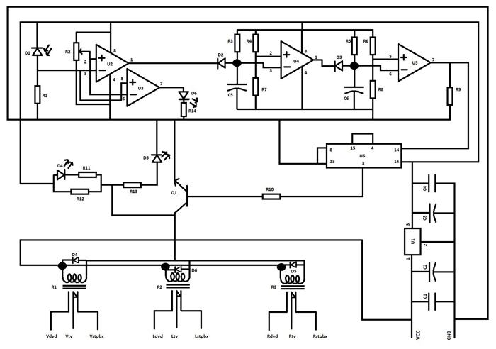
Fig. 96: Circuit Diagram With All Connections Of Functional Block
External DC supply of 9V, 5A is suitable to provide VCC and GND for this circuit design
The components used in this circuit and their details are listed in the following table
|
Serial no. |
COMPONENT |
TYPE |
VALUE |
|
1 |
D1 |
IR Photodiode |
directional IR photodiode |
|
2 |
R1 |
Resistor |
100KE |
|
3 |
R2 |
Variable resistor |
10KE |
|
4 |
U2 |
Op-amp |
½ LM358 |
|
5 |
U3 |
Op-amp |
½ LM358 |
|
6 |
R3 |
resistor |
270 KE |
|
7 |
R4 |
resistor |
1 KE |
|
8 |
R7 |
resistor |
1 KE |
|
9 |
C5 |
Capacitor |
1 mfd |
|
10 |
D2 |
Diode |
1N4007 |
|
11 |
U4 |
Op-amp |
½ LM358 |
|
12 |
R6 |
resistor |
1 KE |
|
13 |
R8 |
resistor |
1 KE |
|
14 |
R5 |
resistor |
270 KE |
|
15 |
C6 |
Capacitor |
100 mfd |
|
16 |
D3 |
Diode |
1N4007 |
|
17 |
U5 |
Op-amp |
½ LM358 |
|
18 |
U6 |
DECADE COUNTER |
CD4017 |
|
19 |
Q1 |
NPN TRANSISTOR |
SL100 |
|
20 |
R10 |
RESISTOR |
550 E |
|
21 |
R11 |
RESISTOR |
1 KE |
|
22 |
R13 |
RESISTOR |
1 KE |
|
23 |
D4 |
LED |
RED |
|
24 |
D5 |
LED |
YELLOW |
|
25 |
D6 |
LED |
RED |
|
26 |
R14 |
RESISTOR |
1 KE |
|
27 |
C1 |
CAPACITOR |
0.1 mfd |
|
28 |
C2 |
CAPACITOR |
1000 mfd |
|
29 |
C3 |
CAPACITOR |
1000 mfd |
|
30 |
C4 |
CAPACITOR |
0.1 mfd |
|
31 |
U1 |
POSITIVE DC REGULATOR |
7805 |
|
32 |
RL1 |
RELAY |
6 V |
|
33 |
RL2 |
RELAY |
6 V |
|
34 |
RL3 |
RELAY |
6 V |
|
35 |
D4 |
DIODE |
1N4007 |
|
36 |
D5 |
DIODE |
1N4007 |
|
37 |
D6 |
DIODE |
1N4007 |
|
38 |
R9 |
RESISTOR |
1 KE |
|
39 |
R12 |
RESISTOR |
1 KE |
Fig. 97: Component Details Of The Complete Circuit Diagram
The functions of the entire components used in this circuit are listed in the following table
|
COMPONENT |
FUNCTION |
|
D1 |
The photodiode for sensing the incoming IR light rays |
|
R1 |
The resistor acts as a pull down resistor with the photodiode and is used for biasing the photodiode. Increases the resistance will increase the sensitivity up to certain extend. |
|
R2 |
This is a variable resistor and is use to set the voltage level above which the voltage from the IR PHOTODIODE block needed to be detected by the op-amps. |
|
U2 |
This op-amp is used for the level detection of input from the IR PHOTODODE block and produces an output for the MONOSTABLE SMALL block. It compares the voltage from the IR PHOTODIODE block and whenever the voltage is above the voltage level set by the resistor R2, the output become high |
|
U3 |
This op-amp is used for the level detection of input from the IR PHOTODODE block and produces an output for the IR INDICATOR block. It compares the voltage from the IR PHOTODIODE block and whenever the voltage is above the voltage level set by the resistor R2, the output become high |
|
R4 |
The R4 forms a potential divider network with the R7 and the R4 connects the VCC to the potential divider network. The output from the potential divider network is taken from the point where the R4 connects with the R7. Increasing the value of R4 decreases the voltage output from the potential divider network. |
|
R7 |
The R7 forms a potential divider network with the R4 and the R7 connects the GND to the potential divider network. The output from the potential divider network is taken from the point where the R7 connects with the R4. Increasing the value of R7 increases the voltage output from the potential divider network. |
|
R3 |
The R3 is used along with C5 as an R-C network or a tank circuit. It is through the R3 that the capacitor charges to the input voltage. Increasing the value of the R3 makes the charging process slower and decreasing the value of the R3 makes the charging process faster. |
|
C5 |
The C5 is used along with R3 as an R-C network or a tank circuit. The capacitor C5 charges to the input voltage through the resistor R3. Increase the value of C5 and the capacitor will take more time to charge up to a particular voltage. Hence increasing the value of the C5 makes the charging process slower and decreasing the value of the C5 makes the charging process faster. |
|
U4 |
The U4 is the op-amp used to detect whenever the voltage across the capacitor rises across a predefined value set by the potential divider network. The positive input of the op-amp is connected to the potential divider network and the negative input pin is connected to the output of the R-C network. Whenever the voltage across the capacitor is above the predefined voltage level the output becomes low, otherwise remains high |
|
D3 |
It couples the output from the COMPARATOR block and applies it across the charging capacitor C5. The zero voltage is coupled only and prevents the positive voltages from affecting the charging of the circuit |
|
R6 |
The R6 forms a potential divider network with the R8 and the R6 connects the VCC to the potential divider network. The output from the potential divider network is taken from the point where the R6 connects with the R8. Increasing the value of R4 decreases the voltage output from the potential divider network. |
|
R8 |
The R8 forms a potential divider network with the R6 and the R8 connects the GND to the potential divider network. The output from the potential divider network is taken from the point where the R8 connects with the R6. Increasing the value of R8 increases the voltage output from the potential divider network. |
|
R5 |
The R5 is used along with C6 as an R-C network or a tank circuit. It is through the R5 that the capacitor charges to the input voltage. Increasing the value of the R5 makes the charging process slower and decreasing the value of the R5 makes the charging process faster. |
|
C6 |
The C6 is used along with R5 as an R-C network or a tank circuit. The capacitor C6 charges to the input voltage through the resistor R5. Increase the value of C6 and the capacitor will take more time to charge up to a particular voltage. Hence increasing the value of the C6 makes the charging process slower and decreasing the value of the C6 makes the charging process faster. |
|
U5 |
The U5 is the op-amp used to detect whenever the voltage across the capacitor rises across a predefined value set by the potential divider network. The positive input of the op-amp is connected to the potential divider network and the negative input pin is connected to the output of the R-C network. Whenever the voltage across the capacitor is above the predefined voltage level the output becomes low, otherwise remains high |
|
D3 |
It couples the output from the MONOSTABLE SMALL block and applies it across the charging capacitor C6. The zero voltage is coupled only and prevents the positive voltages from affecting the charging of the circuit |
|
U6 |
This decade counter IC is wired as a bi stable circuit. This bi stable circuit toggles its output state on the rising edge of the input clock pulse |
|
R9 |
This capacitor is used to pull down the input of the bi stable to set a default logic low voltage at the clock input even if there is no deices connected to the bi stable. This resistor prevents false triggering up to an extent in the bi stable. |
|
R10 |
This is the base resistor and is used to set the collector current of the transistor in a required range by controlling the current flowing to the base when a logic high input is applied. Increasing the value of the base resistor decreases the current flowing towards the base and hence decreases the collector current of the transistor. Decreasing the value of the base resistor increases the current flowing towards the base and hence increases the collector current of the transistor |
|
Q1 |
This transistor is used as a power amplifier and is connected in a Class-B power amplifier configuration. It generate an output collector current which is the product of the base current and the current gain of the transistor |
|
D4 |
The D4 glows when the output from the DRIVER block is logic zero voltage. |
|
R11 |
This is the current limiting resistor for the D4 LED and it controls the current flowing through the LED when it is ON. Increasing the value of the resistor will decrease the current flowing through the D4 LED and hence reduces its brightness and decreasing the value of resistance will increase the current flow and hence increases the brightness. |
|
D5 |
The D5 glows when the output from the DRIVER block is logic high voltage. |
|
R13 |
This is the current limiting resistor for the D5 LED and it controls the current flowing through the LED when it is ON. Increasing the value of the resistor will decrease the current flowing through the D4 LED and hence reduces its brightness and decreasing the value of resistance will increase the current flow and hence increases the brightness. |
|
R12 |
This resistor is used to pull up the input of the RELAY INDICATOR circuit so that there will be a default voltage even if there is no device connected to the input of the circuit. |
|
D6 |
The D6 glows when the output from the COMPARATOR block is logic high voltage. |
|
R14 |
This is the current limiting resistor for the D6 LED and it controls the current flowing through the LED when it is ON. Increasing the value of the resistor will decrease the current flowing through the D6 LED and hence reduces its brightness and decreasing the value of resistance will increase the current flow and hence increases the brightness. |
|
C1 |
This capacitor is called bypass capacitor and is used to bypass very short duration spikes to the ground without affecting the other components. |
|
C2 |
This is the filter capacitor used to stabilize the slow variations in the input voltage to the circuit. Increasing the value of the capacitor increase the stabilization and decreasing the value of the capacitor decreases the stabilization. However this capacitor is not good enough to check very narrow duration spikes appears at the input. |
|
C3 |
This is the filter capacitor used to stabilize the slow variations in the output voltage from the circuit. Increasing the value of the capacitor increase the stabilization and decreasing the value of the capacitor decreases the stabilization. However this capacitor is not good enough to check very narrow duration spikes occurs at the output. |
|
C4 |
This capacitor is called bypass capacitor and is used to bypass very short duration spikes to the ground without affecting the other components |
|
U1 |
This is the positive DC regulator IC and it can maintain the output voltage constant precisely at a particular value even though there are significant variations in the input voltage. |
|
RL1 |
The common lead of this relay is connected to the video input of the TV, NO lead is connected to the video output from the DVD player and the NC lead is connected to the video output from the DTH set top box. It is hence used to switch the video signals from the DVD and DTH to the TV. |
|
RL2 |
The common lead of this relay is connected to the left audio input of the TV, NO lead is connected to the left audio output from the DVD player and the NC lead is connected to the left audio output from the DTH set top box. It is hence used to switch the left audio signals from the DVD and DTH to the TV. |
|
RL3 |
The common lead of this relay is connected to the right audio input of the TV, NO lead is connected to the right audio output from the DVD player and the NC lead is connected to the right audio output from the DTH set top box. It is hence used to switch the right audio signals from the DVD and DTH to the TV. |
|
D4 |
This is the freewheeling diode use to prevent the back EMF generated by the RL1 from affecting other circuits. |
|
D6 |
This is the freewheeling diode use to prevent the back EMF generated by the RL2 from affecting other circuits. |
|
D5 |
This is the freewheeling diode use to prevent the back EMF generated by the RL3 from affecting other circuits. |
Fig. 98: Component Functions In The Complete Circuit Diagram
Finally we have a circuit diagram for our device and now we are ready to build the circuit. Let us quickly finish the next step in which we will make a list of the components required with their specifications so that we have all the required components with us before we actually start building something.
Step: 7) Make a Bill of Materials (BOM)
The list of the components required with their details and specifications should be made as a list so that it is easy to purchase the required components. It also helps us to estimate the cost of the materials. We should have all the required components with us before we actually start building the modules. The BOM of the complete circuit diagram is given in the following table.
|
COMPONENT |
VALUE |
SPECIFICATION |
QUANTITY |
|
IR Photodiode |
Directional IR photodiode |
Glass type IR LED receiver |
1 |
|
Resistor |
100KE |
¼ Watt, carbon film |
1 |
|
Resistor |
270 KE |
¼ Watt, carbon film |
2 |
|
Resistor |
1 KE |
¼ Watt, carbon film |
9 |
|
Resistor |
550 E |
¼ Watt, carbon film |
1 |
|
Variable resistor |
10KE |
¼ Watt, carbon film |
1 |
|
Op-amp |
LM358 |
Dual op-amp single supply |
2 |
|
Diode |
1N4007 |
1 Ampere, general purpose rectifier |
5 |
|
Capacitor |
1 mfd |
16V, electrolytic |
1 |
|
Capacitor |
100 mfd |
16V, electrolytic |
1 |
|
CAPACITOR |
0.1 mfd |
Ceramic disc type |
2 |
|
CAPACITOR |
1000 mfd |
16V, electrolytic |
2 |
|
LED |
Red |
3mm LED |
2 |
|
LED |
Yellow |
3mm LED |
1 |
|
RELAY |
6 V |
¼ Watt, carbon film |
3 |
|
DECADE COUNTER |
CD4017 |
Decade counter |
1 |
|
NPN TRANSISTOR |
SL100 |
NPN general purpose |
1 |
|
POSITIVE DC REGULATOR |
7805 |
Positive DC regulator |
1 |
Fig. 99: The BOM Of The Circuit
Note that the above BOM is based on the components found in the circuit diagram only; connectors, wires, circuit board etc. are excluded.
We have the circuit diagram, we have the BOM and hence we are all set for the actual hardware making process. Let us start with the step in which we identify which all parts in our circuit can be made into reusable modules. Reusable modules are electronic hardware which can be directly plug in and out on to other circuit boards without any modifications and have some defined pin outs and functions.
Filed Under: Circuit Design


Questions related to this article?
👉Ask and discuss on Electro-Tech-Online.com and EDAboard.com forums.
Tell Us What You Think!!
You must be logged in to post a comment.