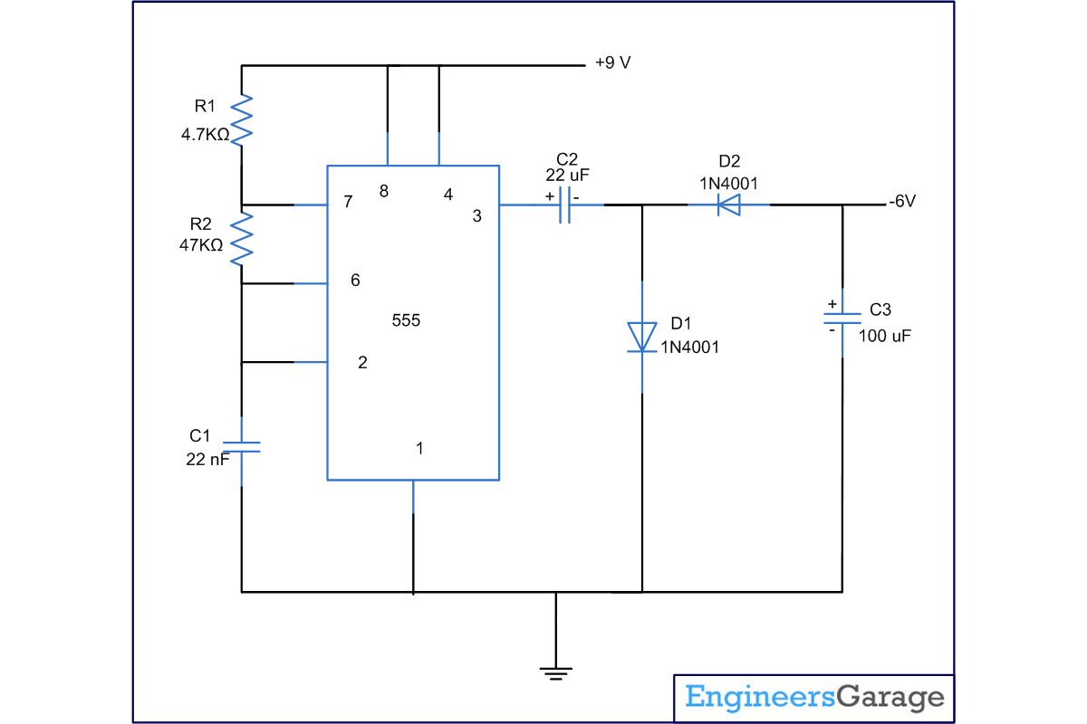
This circuit and project demonstrates the application of 555 to generate negative supply. The negative supply produced is about 3 volts lesser than the applied voltage due to various losses. At times the circuit requires both negative and positive supply, which is not available in the batteries.Image below shows the pin diagram of a standard 555 IC:
[[wysiwyg_imageupload:7742:]]
Fig. 1: Pin Diagram of a Standard 555 IC
In this project, 555 works in astable mode and produces a frequency of about 663 hertz. This frequency is taken at output pin (pin3) of 555.The circuit connected at pin3 works to combine voltages at positive and negative cycles, and then adding them to give the net output. During positive cycle D2 gets reverse biased, so C3 could not be charged while D1 becomes forward biased, charging capacitor
C2. During the negative pulse D1 becomes reverse biased and D2 becomes forward biased, thereby charging capacitor C3.The voltage of both add up giving us negative voltage of about 6V. The loss takes place in various steps. Firstly the output pin rises to about 1.7 volts less than Vcc voltage plus some losses occur in power diodes too leading to total loss of about 3 volts. Here output current must be kept near to 50 mA; otherwise output voltage will drop further.
Circuit Diagrams
Project Components
Filed Under: 555 Timers, Electronic Projects

Questions related to this article?
👉Ask and discuss on Electro-Tech-Online.com and EDAboard.com forums.
Tell Us What You Think!!
You must be logged in to post a comment.