Simulations and prototyping have been a very important part of the electronics industry since a very long time now. Before heading in for the actual fabrication of a dedicated hardware, everyone would want to be sure that what they are making will work the way they want it to. Over all these years while electronics companies offered dedicated hardware in their products, it was not possible for the end user to reconfigure them to his own needs. This need led to the growth of a new market segment of customer configurable Field Programmable integrated circuits called Field Programmable Gate Arrays or FPGAs.
History

Fig. 1: A Representational Image Of Field Programmable Gate Arrays
The FPGA share a common history with most Programmable Logic Devices. The first of this kind of devices was the Programmable Read Only Memory. Further driven by need of specifically implementing logic circuits, Philips invented the Field-Programmable Logic Array (FPLA) in the 1970s. This consisted of two planes, a programmable wired AND-plane and the other as wired OR. It could implement functions in the Sum of Products form.
To overcome difficulties of cost and speed, Programmable Array Logics were developed which had only one programmable ‘AND’ plane fed into fixed OR gates. PALs and PLAs along with other variants are grouped as Simple Programmable Logic Devices (SPLDs). In order to cater to growing technological demands, SPLDs were integrated onto a single chip and interconnects were provided to programmably connect the SPLD blocks. These were called Complex PLDs and were first pioneered by Altera, the first in the family being Classic EPLDs and then, MAX series.
Then another class of Electronic devices, Mask-Programmable Gate Arrays consisting of transistor arrays which could be connected using custom wires motivated the design of the FPGAs. Transistors gave way to Logic Blocks and the customization could now be performed by the user on the field and not in the manufacturing lab. The credit to develop the first commercially viable FPGA goes to Xilinx co-founders Ross Freeman and Bernard Vonderschmitt. The XC2064 was invented in 1985 consisting of 64 Configurable Logic Blocks with 3 Look Up Tables. It was in late 1980s when Steve Casselman’s proposed experiment to implement a computer with 6,00,000 reprogrammable gates found sponsors in US Naval Surface Warfare department and later a patent in 1992.
By the end of 1990, a lot of competition sprung up in manufacturing FPGAs when Xilinx’s market share started to decline. Players like Actel, Altera, Lattice, QuickLogic, Cypress, Lucent and SiliconBlue started entering this field and carving their niche in the world FPGA Market along with Xilinx, as FPGA started gaining acceptance in applications like Digital Signal Processing and Telecommunications. In 1997, Adrian Thompson succeeded in merging a genetic algorithm technology with FPGA and started a new age of Evolvable hardware.
Programming Technologies
FPGA’s can be considered to be building bricks which allow desired customization of the hardware. These are a special form of PLDs with higher densities and with increased capability of implementing functionality in a shorter time span using CAD. The FPGA’s are available in various flavours based on the programming technology used. These may be programmed using:
1. Antifuse Technology, which can be programmed only once. Devices manufactured by QuickLogic are examples of this type. Configuration is done by burning a set of fuses. These act as replacements for Application Specific ICs (ASIC) and used in places where protection of intellectual property is top priority.
2. Flash Technology based Programming, like devices from Actel. The FPGA may be reprogrammed several thousand times, taking a few minutes in the field itself for reprogramming and has non-volatile memory.
3. SRAM Technology based FPGAs, the currently dominating technology offering unlimited reprogramming and very fast reconfiguration and even partial reconfiguration during operation itself with little additional circuitry. Most companies like Altera, Actel, Atmel and Xilinx manufacture such devices.
Configurable Logic Blocks
Irrespective of the different manufacturers and slightly different architectures and feature sets, most of the FPGA’s have a common generic approach. The main component blocks of any FPGA are a flexible programmable ‘Configurable Logic Block’ (CLB), surrounded by programmable ‘Input/ Output Blocks’ with a hierarchy of routing channels interconnecting various blocks on the board. Additionally, these may consist of Clock DLLs for clock distribution and control and Dedicated Block RAM memories. 

Fig. 2: Figure Showing Flexible Programmable Configurable Logic Block Of Any FPGA
Configurable Logic Block
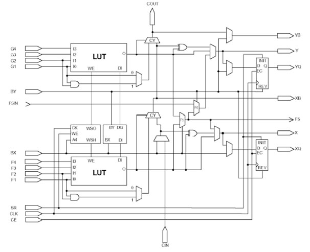
The basic building block of a Configurable Logic Block is the logic cell. A logic cell may consist of an input function generator, carry logic and a storage element. The function generators are implemented as Look Up Tables depending on the input. For example, a Xilinx Spartan II has 4 inputs LUT where each LUT can provide a 16X1 bit Synchronous RAM which can be further multiplexed using multiplexers. An LUT may also be used as a Shift register which is used to capture burst-mode data. The storage elements may be used as edge sensitive flip-flops or level sensitive latches. The arithmetic logic includes an XOR gate for full adder operation along with dedicated carry logic lines. The figure below shows an FPGA slice:

Fig. 3: Figure Showing FPGA Slice
I/O Block & Routing Matrix
Input/ Output Block
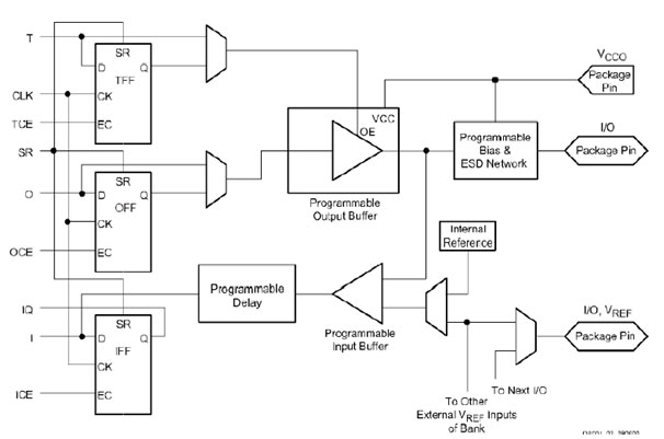
This block features inputs and outputs supporting a wide range of signaling standards and interfaces. A basic Input/ Output block is shown below:

Fig. 4: Logic Gate Diagram Of Basic Input Output And Routing Matrix In FPGA
The buffers in the Input and output paths route the input and output signals to the internal logic and the output pads either directly or via a flip-flop. The buffer can be set to conform to various supported signaling standards which might even be user defined and externally set.
Routing Matrix
In any assembly line it is often the slowest segment which sets the overall production rate. Much in the same way, it is the route that takes the longest delay that eventually determines the performance of the entire electronic system. Thus routing algorithms are brought into place for the design of the most efficient paths to deliver optimum performance. Routing is on various levels like Local, between LUTs, flip-flops and the General Routing Matrix, General Purpose Routing between various CLBs, I/O Routing between I/O Blocks and CLBs, Dedicated Routing for a certain classes of signals for maximizing performance and Global Routing for distributing clocks and other signals with very high fanout.
Clock Distribution
High speed, low skew clock distribution is provided in most FPGAs using Primary Global Routing resources. With each clock input buffer, there is a digital Delay-Locked Loop which eliminates skew between clock input pad and internal clock input pins by adjusting the delay element, and also provides control of multiple clock domains.
FPGA families now also have large block RAM structures to complement the distributed RAM LUTs, size varying for different FPGA devices.
The design of an FPGA follows mostly the same approach as any VLSI system the chief steps being Design Entry, Behavioral Simulation, Synthesis, Post Synthesis Simulation, translation, mapping and routing, and further analysis like Timing simulation and Static Timing Analysis. On a computer, the design looks all ordered and tiled, yet imperfect placement and routing happens and leads to performance drops.
In order to increase the performance of FPGAs, more transistors could always be used. The area overhead involved in FPGAs is higher than ASIC and could possibly do with more density now that 28nm processes are also being implemented on them. Putting more transistors also means that larger designs would be possible. Leakage is a major issue with FPGAs and has been an area of interest. Use of asynchronous FPGA architecture has also shown better results coupled with pipelining technology which reduces global inputs and improves throughput. 

Fig. 5: An Image Showing Pipeline Dataflow in FPGA
Security used to be a major concern as the code needed to be revealed every time it was loaded on to the FPGA’s, thus making FPGA’s flexibility a potential threat to malicious modifications during fabrication. But, bitstream encryption has come to the rescue of FPGAs.
Often the inexperienced designers and users face this dilemma that how much powerful FPGA would be suitable for their application. Manufacturers often specify metrics like ‘Gate count’. For Example, Xilinx uses 3 metrics to measure capacity of FPGA, Maximum Logic Gates, Maximum Memory Bits and Typical Gate Range. As long as these quoted metrics are consistent, migration between families is somewhat simplified, but it rarely offers subtle comparison between different vendors because of the difference of architectures and as a result of which, performance varies. A better metric is to compare the type and number of logic resources provided. In addition to it, the designer must be fully aware of what is exactly required of the device as vendors might be boasting of features which would be of least importance to the job. For example, Altera’s Stratix II EP2S180 features about 1,86,576 4-Input LUTs while Xilinx Virtex-4 XC4VLX200 contains 1,78,176. However if the design needs only 177K LUTs, the latter would suffice. If RAM is the desired metric for the designer, neither the Xilinx XC4VLX200’s 6Mbits nor the Altera’s EP2S180’s 9Mbits would be favoured over the lesser advertised, older model of XC4VFX140 standing at 9.9Mbits. So it requires thorough understanding on the part of the user who finally needs it and not what the newest product on the shelf offers.
Importance of FPGA
FPGA hold promise of delivering even in harsh conditions. The cyclone devices from Altera work well in temperature ranges of -40 degrees to 85 degrees. Another factor that promotes their long term use is the long term availability. ASIC manufacturers do not agree on availability of 5 or at maximum 10 years, where as FPGAs have nearly unlimited availability even if device migrates to next generation.
These find use in microprocessor systems like the PowerPC405 embedded cores, in Digital Signal Processing as embedded multipliers and in I/O Processing like Digitally controlled Impedance. It is always better to be sure of the design and its performance by testing it on FPGA’s before going in for ASIC circuits. These are employed in Defense systems and medical imaging. The possibility of evolvable hardware was revealed while implementing speech recognition on an FPGA using genetic algorithm. FPGAs being parallel processing devices find use in applications like brute force attacks used in breaking cryptographic algorithms, in convolution and FFT computations.
Future
With the improvement in software tools for FPGA development, primarily by the traditional vendors and also independent tool vendors like Synplicity, FPGA is becoming more popular day by day. Now, FPGAs have started including specialized hardware of customer needed functions, reducing costs to manufacturers. Thus the future might see a competition between hard-core low cost systems or soft-core tweekable systems. The costs are expected to lower even more in the near future as FPGA’s popularity continues to grow manifold. Vendors have starting experimenting with concepts like embedding FPGA inside ASICs making a hybrid device. Focus continues to be on the interconnect routing and lesser changes are observed in the architectures of CLBs. As FPGAs continue to incorporate processors, the newer generation of FPGAs would require not only the hardware knowledge of digital design but also require software expertise on the part of the designer. All in all, the FPGAs are expected to take away the market share from ASIC devices and become a dominant technology engulfing a plethora of applications from diversified fields.
Filed Under: Articles


Questions related to this article?
👉Ask and discuss on EDAboard.com and Electro-Tech-Online.com forums.
Tell Us What You Think!!
You must be logged in to post a comment.