A field-programmable gate array or FPGA is a logic chip that contains a two-dimensional array of cells and programmable switches. Essentially, they’re integrated circuits (ICs) that have an array of identical logic blocks with programmable interconnections.
Similar to how you can paint any picture on a blank canvas, an FPGA lets an engineer design any digital circuit. Simply generate and download the bit file, and you’re good to go.
This is a significant development compared to conventional microcontrollers, which fail to support larger designs. For example, the 8051 microcontrollers used Harvard architecture with CISC’s instruction set. FPGAs do not have such inbuilt instruction sets, providing the designer with greater flexibility.
Another difference: where a microcontroller has its own CPU that starts the controller, retains memory, and performs several tasks, an FPGA does not. It’s unable to start functioning on its own because of this lack of traditional architecture.

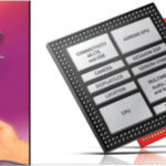
Illustration of a typical FPGA device.
Why FPGAs?
Compared to a microcontroller, FPGAs offer several advantages. As mentioned, they’re far more flexible than the limited functionality of controllers. FPGAs also have greater higher memory capacity.
The primary difference between the two is that an FPGA controls hardware whereas a microcontroller controls software. This is why the FPGA is typically programmed in the hardware descriptive languages (HDLs).
There are technologies that are similar to the FPGA, although with different applications, gates, and basic architectures. For example, application-specific integrated circuits (ASICs) are also programmed by HDLs. The difference is that they’re designed for one particular application whereas FPGAs offer the freedom to execute any design.
The advantage of ASICs is that they run faster. But FPGAs can act like ASICs, which is a plus. FPGAs also have the ability to reprogram in the case of a bug. ASICs are unable to do so.
Another similar technology is found in complex programmable logic devices (CPLDs). CPLDs have the characteristics of programmable logic arrays (PALs) and FPGAs.
Here’s a comparison between the two:
1. CPLDs have non-volatile memory whereas FPGAs have volatile memory. This means on “Power-ON,” a CPLD retains memory, whereas an FPGA deletes previous data. This is why an FPGA requires an external ROM. Previous data is, then, provided to the FPGA when powered on.
2. The primary element of a CPLD is a macrocell. A single macrocell consists of several AND gates, a D flip-flop, a multiplexer, and an EX-OR gate. They’re connected using a block called, a programmable interconnect. The main element of an FPGA is a look-up table or LUT.In a Xilinx device, the LUT is a function generator that can provide 16×1 bit synchronous RAM and ROM. Function generators are implemented as 4 input LUTs.
3. A CPLD has about 500 to 12,000 gates, which is a much fewer number than an FPGA. It has between 3,000 to 5,00,000 gates.
4. The cost of an FPGA is higher than that of a CPLD.
An FPGA is often preferred, offering more flexibility with a greater number of gates. These features matter when designing complex circuits.
FPGA architecture
The main blocks of any architecture are configurable logic blocks (CLBs) or logic blocks, interconnect, and I/O lines. Here’s an illustration of the FPGA:

The architecture of an FPGA.
A CLB is the basic building block of an FPGA. It’s a logic cell that can be configured or programmed to perform specific functions. These building blocks are connected to the interconnect block.
A CLB can be implemented using LUT or multiplexer-based logic. In LUT-based logic, the block consists of a look-up table, a D flip-flop, and a 2:1 multiplexer. Flip flops are used as storage elements. The multiplexer selects the appropriate output.
Each CLB is made up of a certain number of slices. Slices are grouped in pairs and arranged in columns. The number of CLBs in a device varies, according to the vendor and the family of the device. For example, Xilinx’s Spartan 3E FPGA contains four slices. Each slice is made up of two LUTs and two storage elements.
The function of the LUT is to implement logic, whereas the dedicated storage elements can be flip-flops or latches. The CLBs are arranged in an array of rows and columns.

Illustration of an FPGA building block, using a LUT-based CLB.

Illustration of an FPGA building block, using an MUX-based CLB.

The arrangement of CLBs in the Spartan3E FPGA.
The interconnect is the programmable network of signal pathways existing between the inputs and outputs of a device’s functional elements. This is also known as routing.
There are several types of routing including local routing for interconnection between:
- LUTs
- Flip-flops and general routing matrix
- General-purpose routing for interconnection between the rows and columns of CLBs
- I/O routing for the purpose of pin-swapping or locking
Routing options allow for the adoption of new designs to the existing PCB layout. Other routing methods include dedicated routing sources to improve performance, the global routing distributed clock, and other signals.

A cross-sectional diagram of a direct interconnect technique used in FPGA devices.
Input/output blocks (IOBs) offer programmable unidirectional or bidirectional interfaces between the package pins and the device’s internal logic.
There are three signals present within an IOB:
1. The input path to carry data from the pad to the respective line.
2. The output path that carries data from the internal logic to the IOB pad via a multiplexer and a three-state driver.
3. The three-state path, which determines the output driver’s state of high impedance
All of the signals come with the option of an inverter.
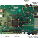
A Spartan2 FPGA input/output block.
Distributed and block RAM
Distributed and block RAM are mostly found in Xilinx devices. Most of the configurable logic blocks or CLBs in a Xilinx device contain a small amount of RAM that’s a single or double port. It’s called distributed RAM because it’s spread throughout the FPGA over several LUTs.
A disadvantage of distributed RAM is that it cannot be used for larger designs since a single CLB is insufficient. However, it’s possible to implement several block RAMs in parallel for greater memory. The Xilinx synthesizer tool infers which type of memory to use based on the code.
Block memory is a dedicated block of two-port memory, consisting of several kilobytes of RAM. It should be implemented in larger devices. The number of block RAMs present in an FPGA depends on how advanced it is. For example, the Spartan 6 FPGA has a larger-sized block of RAM than the Spartan 3.
Distributed and block RAM have different modes of operation. Although the WRITE operation for each one is synchronous, the READ operation varies. For distributed RAM, data is read directly as soon as it is entered, meaning it does not wait for the clock signal. This means it is asynchronous.
On the other hand, block RAM operates on a synchronous mode of operation, so data can be written into the memory only at the rising edge of the clock.
The implementation style can select either type of RAM by using the “ram_style” constraint.
Programming an FPGA
The languages that can be used to program an FPGA are VHDL, Verilog, and SystemVerilog.
Very high-speed integrated circuit (VHSIC) hardware description language (VHDL) has all of the features that real-life hardware possesses.
The key features of VHDL include that it’s:
- A concurrent language, meaning that statements can be implemented in a parallel manner, similar to real-life hardware.
- A sequential language, meaning that statements are implemented one after another in a sequence.
- A timing-specific language. The signals, much like clocks, can be manipulated as per a specific requirement. For example, you can start a process when the clock is on the rising edge, providing adequate delay, inverting the clock, etc.
- Not case sensitive. The VHDL code is translated into wires and gates that are mapped onto the device.
The different modeling styles of the VHDL include behavioral, structural, dataflow, and a combination of all three.
Combinational and sequential statements can be used to implement the modeling styles. Sequential statements are implemented one after another (serially), whereas combinational statements are executed simultaneously (in a parallel manner).
In the behavioral style, only the functions are described, typically by using the PROCESS statement. The architecture of registers is not defined.
In the structural type, the circuit is described in terms of the interconnected components. For example, a full adder is implemented in terms of two half-adders.
In the dataflow style, the circuit is described using concurrent statements. So, a MUX could be described in terms of gates, such as EXOR — implemented as per the Boolean expression obtained from the truth table. (Although this is not an ideal way of writing code because it has several dependencies and uses concurrent statements.)
Mixed modeling styles use any combination of these three styles.
CODE: A behavioral implementation of a 4-bit counter in VHDL
library IEEE;
use IEEE.STD_LOGIC_1164.ALL;
use IEEE.STD_LOGIC_ARITH.ALL;
use IEEE.STD_LOGIC_UNSIGNED.ALL;
use work.display.all;
entity counter is
Port ( clk : in STD_LOGIC;
out_count : out STD_LOGIC_VECTOR (3 downto 0));
end counter;
architecture Behavioral of counter is
begin
process(clk)
variable count:std_logic_vector(3 downto 0):=”0000″;
begin
if(clk’event and clk=’1′) then
count:=count+’1′;
if(count=”1111″) then
count:=”0000″;
end if;
end if;
out_count<=count;
end process;
end Behavioral;

Schematic of a register-transfer level or RTL.
Verilog is also a hardware descriptive language (HDL) that’s typically used to design and verify digital circuits and the register-transfer level or RTL (meaning how data is transformed as it’s passed from register to register) of abstraction. So, it allows designs at various levels of abstraction. It has a C-like syntax.

An example of how the Verilog language defines hardware in FPGA devices.
Verilog has three levels of abstraction: behavioral, RTL, and gate-level.
In the behavioral abstraction, a system is described by a concurrent algorithm. In the RTL, the system is implemented by transferring data between the registers with respect to the clock. In the gate level of abstraction, a system is characterized by the timing and logical links.
The Verilog system is built by modules and ports. The modules contain various components and may consist of instances of other modules. The ports have three types: input, output, and inout.
The modules include:
1. Parameters: constants with a value that’s specified at the time of compilation.
2. Nets: connect components.
3. Registers: serve as storage elements, with values stored during the procedural statements. (The types of registers are reg, integer, type, and real.)
4. Primitives and instances: pre-defined module types, such as the logical gates.
5. Continuous assignments: describe how data moves from one place to another (from a net or a register).
6. Procedural blocks: represent sequential behavior — these are sequences of executable statements.
7. Task/function definitions: implemented only within a procedural block.

The hierarchy of a Verilog system.
VHDL versus Verilog
The VHDL and Verilog languages are equally effective in terms of hardware descriptions. Typically, selection is based on preference, the available electronic design automation (EDA) tools, and the commercial, business, and marketing goals.
VHDL allows for the compilation of multiple design units to reside in the same file, which is useful when managing large design structures. It’s ideal for high-level hardware modeling, offering several libraries.
In terms of datatypes, VHDL offers a wide choice of datatypes (user-defined and otherwise). In Verilog, all of the datatypes are pre-defined. Despite this drawback, Verilog datatypes are easy-to-use and are focused on the modeling aspect of hardware rather than the abstract.
In Verilog, a compilation is usually used to speed up the simulation. This language is favored for its simplicity but it does not offer libraries.
Overall, VHDL is ideal for managing large designs with the help of configuration, generate generic, and package. Verilog has no statements all help manage large design structures. Verilog exhibits C-like features with no statements, but is easier for beginners to learn than VHDL.
FPGA applications
FPGAs are flexible and customizable, making them suitable for a range of high-level industries, such as aerospace, automotive, energy, medical, and defense. For instance, multinational technology conglomerate, Cisco, which manufactures networking hardware and software, uses FPGA in its switches and routers to increase hardware speed.
FPGA is also used in portable electronics, digital signal processing (DSP), and radio astronomy, where it offers high-quality, computational performance compared to microprocessors or DSPs. They’re also found in wireless communication systems, security systems, scientific instruments, and high-performance computing.
In the medical field, FPGAs are currently used in CT scanners, MRIs, ultrasounds, X-ray machines, and surgical systems.
FPGAs offer potential use in nuclear power plants because the systems can be made simpler, easier to test, and more reliable than complex software. Additionally, FPGA-based systems are starting to be used in new plant and I&C (instrumentation and control) designs, as well as in replacements and upgrades for operating plants.
You may also like:
Filed Under: 8051 Microcontroller., Tech Articles
