In the previous tutorial, gate level minimization of boolean functions was discussed. A boolean function must be expressed in standard form as either sum of products (SoP) or product of sums (PoS). Once a boolean function in case is minimized to SoP or PoS form, it can be easily fabricated as two-level implementation of AND and OR gates. A two-level implementation is preferred so that there is minimum delay in signal propagation through logic gates from input to output of the digital circuit.
Practically, digital circuits are constructed with NAND or NOR gates rather than AND or OR gates. The NAND and NOR gates are easy to fabricate with semiconductor components. These are the universal gates from which all other logic gates can be constructed. That is why, all the digital ICs are constructed with NAND or NOR gate rather than other logic gates.
NAND as Universal Gate –
NAND is a universal gate. All other logic gates can be constructed by the NAND gate. A NOT gate can be constructed by one-input NAND gate. A single input NAND gate works same as inverter or NOT gate. The AND gate can be implemented by connecting a NAND gate to a single-input NAND gate where single input NAND gate will work as inverter or NOT gate. The OR gate can be implemented by connecting inputs to single input NAND gates acting as inverter which then connect to a NAND gate. The implementation of AND, OR, and NOT gates with the help of NAND gate is shown in the following logic gate diagrams –
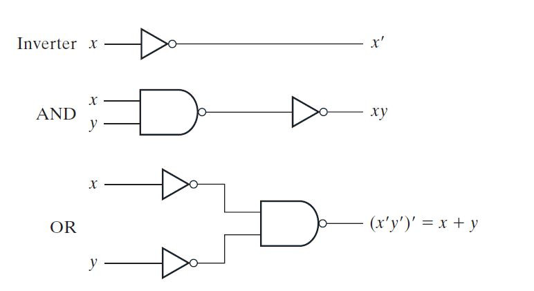
Fig. 1: Image showing Implementation of AND, OR and Invert with NAND Gate
Two-Level Implementation with NAND Gate –
For two-level implementation of a boolean function with NAND gate, it must be expressed in sum of products form. The AND operation (product) between boolean variables (binary data paths) can be implemented by connecting the inputs to a NAND gate which should be connected to a single input NAND gate acting as inverter. The OR operation (sum) can be implemented by connecting the outputs from level 1 to single input NAND gates acting as inverters which should be connected to a NAND gate. Since the complement of a complement of a boolean variable is its normal form, the single input NAND gates at the output of level 1 and at the input of level 2 on same lines can be removed. Therefore, a sum of product expression can be implemented by NAND gates by simple NAND-NAND implementation.
Suppose, a four-variable boolean function F is as follow –
F = AB + CD
In AND-OR implementation, its logic gate diagram will be as follow –
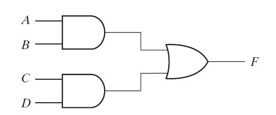
Fig. 2: Image showing Two-Level AND-OR Implementation before NAND-NAND Implementation
A NAND gate can be either shown as AND-Invert or Invert-OR as they are equivalent. The following graphic symbols can be used for NAND gate –

Fig. 3: Symbols of NAND Gate
On replacing the AND plus OR gate by NAND gate in the implementation of the function F, the following logic diagram is obtained –
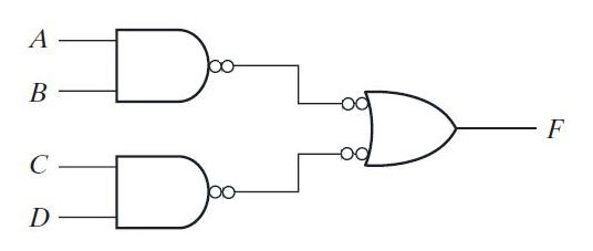
Fig. 4: Image showing Replacement of AND-OR Gates by NAND Gate
As mentioned above the complement of a complement of a boolean variable is its normal form, the single input NAND gates at the output of level 1 and at the input of level 2 on same lines can be removed. So, After removing even number of inverters on same line, the final NAND-NAND implementation of the function will be as follow –
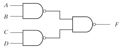
Fig. 5: Image showing Two-Level NAND-NAND Implementation of a Sum of Product Expression
Multi-Level Implementation with NAND Gate –
The gating structure of a digital circuit need not be always feasible to be implemented at two levels. Many times, due to design limitations or for feasibility of the fabrication of an IC, there may require to implement the logic gate diagram of a digital circuit in three or four levels. here are also some boolean functions like Ex-OR which can only be implemented in 3-level or more gate structure. In such case, the boolean function must be first expressed in terms of AND, OR and NOT gates. A logic gate diagram with AND, OR and NOT gates must be drawn and the AND, OR and NOT gates must be replaced by their NAND equivalents. Now, the even number of bubbles (denoting NOT in the NAND Gate) on the same lines must be removed and the remaining single bubbles on lines must be replaced by single input NAND gates. The left is the all-NAND logic gate diagram of the digital circuit.
NOR as Universal Gate –
NOR is also a universal gate like the NAND gate. All other logic gates can be constructed by the NOR gate too. A NOT gate can be constructed by one-input NOR gate. A single input NOR gate works same as inverter or NOT gate. The OR gate can be implemented by connecting a NOR gate to a single-input NOR gate where single input NOR gate will work as inverter or NOT gate. The AND gate can be implemented by connecting inputs to single input NOR gates acting as inverter which then connect to a NOR gate. The implementation of other gates with NOR gate is the dual of the implementation of other gates with the NAND gate. The implementation of AND, OR and NOT gates with the help of NOR gate is shown in the following logic gate diagrams –
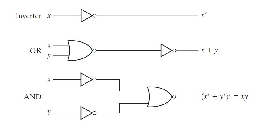
Fig. 6: Image showing Implementation of AND, OR and Invert with NOR Gate
Two-Level Implementation with NOR Gate –
For two-level implementation of a boolean function with NOR gate, it must be expressed in product of sums form. The NOR gate implementation of the AND, OR and NOT gate is just the dual of their NAND gate implementation. The OR operation (sum) between boolean variables (binary data paths) can be implemented by connecting the inputs to a NOR gate which should be connected to a single input NOR gate acting as inverter. The AND operation (product) can be implemented by connecting the outputs from level 1 to single input NOR gates acting as inverters which should be connected to another NOR gate. Since the complement of a complement of a boolean variable is its normal form, the single input NOR gates at the output of level 1 and at the input of level 2 on same lines can be removed. Therefore, a product of sum expression can be implemented by NOR gates by simple NOR-NOR implementation.
Suppose, a four-variable boolean function F is as follow –
F = (A + B)(C + D)
In AND-OR implementation, its logic gate diagram will be as follow –
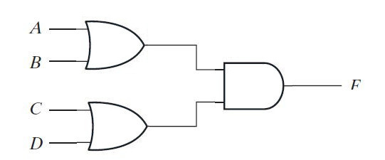
Fig. 7: Image showing Two-Level AND-OR Implementation before NOR-NOR Implementation
A NOR gate can be either shown as OR-Invert or Invert-AND as they are equivalent. The following graphic symbols can be used for NOR gate –

Fig. 8: Symbols of NOR Gate
On replacing the AND, OR and NOT gates by NOR gate in the implementation of the function F, the following logic diagram is obtained –
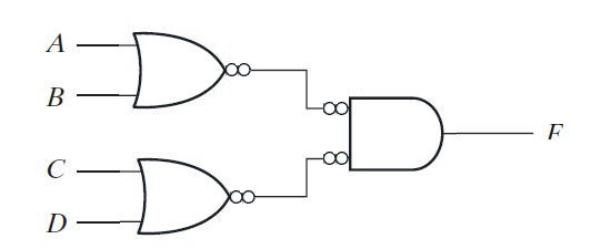
Fig. 9: Image showing Replacement of AND-OR Gates by NOR Gate
As mentioned above the complement of a complement of a boolean variable is its normal form, the single input NOR gates at the output of level 1 and at the input of level 2 on same lines can be removed. So, After removing even number of inverters on same line, the final NOR-NOR implementation of the function will be as follow –
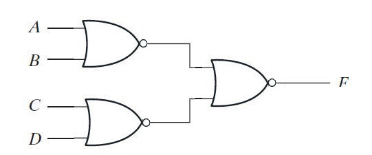
Fig. 10: Image showing Two-Level NOR-NOR Implementation of a Product of Sum Expression
All Possible Two-Level Implementations and Non-degenerate Forms –
Considering two-level implementation of boolean functions and taking AND, OR, NAND and NOR gates available, there can be sixteen possible combinations for two-level implementation of a boolean expression. The eight of these combinations degenerate to single operation, so they are called degenerate forms. The eight degenerate forms are as follow –
1) AND-AND: It degenerates to AND operation. Like if there are four boolean variables A, B, C and D connected in AND-AND gate structure, it will deduce as follow –
F = (AB)(CD)
= ABCD
2) AND-NAND: It degenerates to NAND operation. Like if there are four boolean variables A, B, C and D connected in AND-NAND gate structure, it will deduce as follow –
F = ((AB)(CD))’
= (AB)’ + (CD)’
= A’ + B’ + C’ + D’
= (ABCD)’
3) OR-OR: It degenerates to OR operation. Like if there are four boolean variables A, B, C and D connected in OR-OR gate structure, it will deduce as follow –
F = (A + B) + (C + D)
= A + B + C + D
4) OR-NOR: It degenerates to NOR operation. Like if there are four boolean variables A, B, C and D connected in OR-NOR gate structure, it will deduce as follow –
F = ((A + B) + (C + D))’
= (A + B)'(C + D)’
= A’B’C’D’
= (A + B + C + D)’
5) NAND-OR: It degenerates to NAND operation. Like if there are four boolean variables A, B, C and D connected in NAND-OR gate structure, it will deduce as follow –
F = (AB)’ + (CD)’
= A’ + B’ + C’ + D’
= (ABCD)’
6) NAND-NOR: It degenerates to AND operation. Like if there are four boolean variables A, B, C and D connected in NAND-NOR gate structure, it will deduce as follow –
F = ((AB)’ + (CD)’)’
= (A’ + B’ + C’ + D’)’
= (ABCD)
7) NOR-AND: It degenerates to NOR operation. Like if there are four boolean variables A, B, C and D connected in NOR-AND gate structure, it will deduce as follow –
F = (A + B)'(C + D)’
= A’B’C’D’
= (A + B + C + D)’
8) NOR-NAND: it degenerates to OR operation. Like if there are four boolean variables A, B, C and D connected in NOR-NAND gate structure, it will deduce as follow –
F = ((A + B)'(C + D)’)’
= (A + B) + (C + D)
= A + B + C + D
The remaining eight forms either deduce to sum of products expression or product of sum expression for a boolean function. These are called non-degenerate forms. The eight non-degenerate forms are AND-OR, AND-NOR, OR-AND, OR-NAND, NAND-AND, NAND-NAND, NOR-OR and NOR-NOR. The AND-OR is dual of OR-AND, NAND-NAND is dual of NOR-NOR, NOR-OR is dual of NAND-AND while OR-NAND is dual of AND-NOR and vice-versa. The AND-OR and OR-AND forms are basic forms of a boolean expression. The NAND-NAND and NOR-NOR forms are the universal implementation of any boolean function. The NAND-AND and AND-NOR are equivalent and called AND-OR-Invert implementation. The OR-AND and NOR-OR are also equivalent and called OR-AND-Invert implementation.
AND-OR-Invert Implementation –
Both NAND-AND and AND-NOR perform AND-OR-Invert operation. It is simple AND-OR operation with invert operation implemented at the output. Suppose there are four boolean variables – A, B, C and D, then NAND-AND operation between them will be as follow –
F = (AB)'(CD)’
= (AB + CD)’
Similarly, the AND-NOR operation with four boolean variables – A, B, C and D will deduce as follow –
F = (AB+CD)’
OR-AND-Invert Implementation –
Both OR-NAND and NOR-OR perform OR-AND-Invert operation. It is simple OR-AND operation with invert operation implemented at the output. Suppose there are four boolean variables – A, B, C and D, then OR-NAND operation between them will be as follow –
F = ((A + B)(C + D))’
Similarly, NOR-OR operation with four boolean variables – A, B, C and D will deduce as follow –
F = (A + B)’ + (C + D)’
= ((A + B)(C + D))’
Now, with the knowledge of Gate Level Implementation, any boolean function can be constructed with universal logic gates – NAND and NOR. In the next tutorial, there is a short introduction to VHDL. VHDL is a computer based language that describes the hardware of a digital circuit in textual form. It is a computer based design tool that is extremely helpful in design of large scale digital circuits. The designing of small circuits can be done manually, but large digital circuits require computer based tools for designing. Such tools not only ease the design process, they also reduce the chances of a flawed design.
Filed Under: Digital Electronics, Featured Contributions, Tutorials


Questions related to this article?
👉Ask and discuss on Electro-Tech-Online.com and EDAboard.com forums.
Tell Us What You Think!!
You must be logged in to post a comment.