By Krupa Bhavsar, Applications Engineer, Dialog Semiconductor
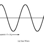
Sine waves are continuous waves, which describe a smooth periodic oscillation. These waves are generally used in signal processing and engineering fields
In this article, dual sine waves with opposite polarity as shown in Figure 1 are generated without coarse PWM “steps”. For generating sine waves, one PWM macrocell is used. The PWM macrocell has pre-programmed table with PWM Duty Cycle values for each sine wave “step”.
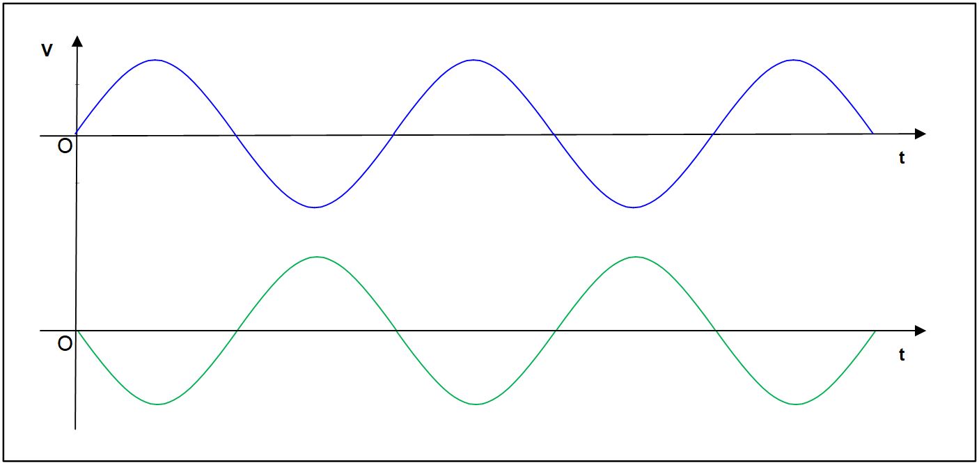
Figure 1. Sine Waves with opposite polarity
This project is divided into three sections. The Clock Frequency Generation section describes calculations to generate new desired sine wave frequency. In the HV PAK section, the circuit design is showed and explained. Finally, the Test Setup and Future Expansion section provides additional details on testing conditions and other possibilities that this project has.
Frequency generation
The sine wave generation is divided into 2 parts. The preprogrammed Duty Cycle values of one part of the wave stored in the PWM macrocell Reg file and steps up after each one clock comes. When the number of clocks is equal to number of Reg file bits, the Up/Down input of the PWM macrocell state changes and Reg file starts to clock in opposite direction.
The new clock frequency generation depends upon sine wave frequency. The number of PWM periods required for a frequency of the sine wave.Equation 1

Where, – desired sine wave frequency, – number of preprogrammed bits, for default is 16.
HVPAK design
 In this project, we used GreenPAK™ circuit to illustrate how the sine wave generator can be built – specifically SLG47105 High Voltage GreenPAK (HVPAK). The complete circuit design file created in the GreenPAK Designer software (available for free) can be found here.
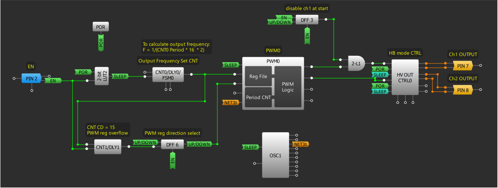
Figure 2 shows the design. This design requires only one external input, i.e. EN input. In this design, PWM0 macrocell is configured as a frequency-controlled generator which generates PWM signal for each part of a sine wave. The outputs of the PWM0 macrocell are connected to HV OUT CTRL0 which is then connected to the external filters to obtain dual sine waves with reverse polarity.
In this project, the HVPAK design is configured to generate a 1kHz sine wave.
The CNT0/DLY0/FSM0 is configured as a Reset Counter. The CNT0/DLY0/FSM0 output period determines a period of each one step of the Reg file and the output sine wave frequency (1).
According to (1) to generate an output sine wave frequency of about 1kHz, CNT0/DLY0/FSM0 output frequency must be equal 31.25kHz or output period 32us.
The direction of PWM changes every 16s clock period. CNT1/DLY1 counts 16 clock periods of the input signal. The DFF6 is configured as a toggle flip-flop which changes the direction of the PWM macrocell.
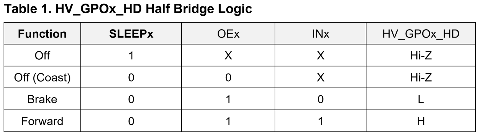
The HV OUT CTRL0 macrocell is configured in Half-Bridge mode control configuration. The PWM0 OUT+ is connected to IN0, and OUT- output is connected to IN1. The OE0 and OE1 inputs are connected to POR. Sleep inputs are used to disable HV OUT CTRL0 when EN signal in Low state.
One pair of external RC filters are required to smooth PWM signals and receive noise-free sine waves.
The DFF3 flip-flop and 2-bit LUT1 are used to skip the first half of the period after the generator start. The first channel sine wave starts from 100% Duty Cycle while the output RC filter is discharged. In this case, half of the first period of the channel 1 sine wave is fully distorted.
So, to generate a sine wave of a desired frequency using a desired input frequency, the designer first calculates the necessary parameters to modify macrocells as described in the Clock Frequency Generation section and then modify the PWM macrocell and CNT settings accordingly as described above.
 Test setup and future expansion
This design is tested using external RC-filters and a push button. The push button is connected to EN input and each RC-filter is connected to HV outputs of HV OUT CTRL0 macrocell as shown in Figure 3. As shown in Figure 4, dual sine wave approximations with opposite polarity are generated when EN input is HIGH.
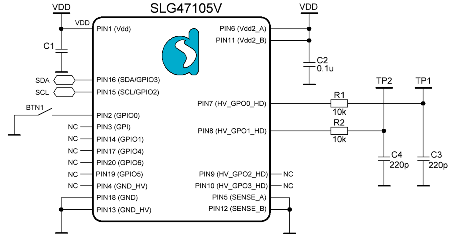
Figure 3. Test Setup
Channel 1 (yellow/top line) – Pin #2 (EN)
Channel 2 (cyan/2nd line) – Sine wave output at Pin #7 (TP1)
Channel 3 (magenta/3rd line) – Sine wave output at Pin #8 (TP2)

Figure 4. Sine Wave Outputs
Future possibilities of this design can be expanded to generate sine waves through an I2C enabled MCU instead of a push button, change sine wave frequency, and also include protection features such as constant current/current limit using Current Sense Comparator and Under-Voltage lockout (UVLO). This design can also be expanded to generate additional dual sine waves by using HV OUT CTRL 1 macrocell.
Conclusion
The HVPAK design described in this article generates two 1kHz sine wave approximations. The design is easy to use, minimizes cost, saves board space and component count.
Moreover, the circuit that we used is quite flexible, easy to test and can accommodate last minute design changes. Once the design is modified, a new design file can be programmed on chip and re-soldered on board. It also offers design security by locking the design file to limit the visibility. By using this design, the user can generate sine waves of desired frequency using PWM macrocells and a single input.
You may also like:


Filed Under: Electronic Projects, Featured, How to

Questions related to this article?
👉Ask and discuss on EDAboard.com and Electro-Tech-Online.com forums.
Tell Us What You Think!!
You must be logged in to post a comment.