Pulse Width Modulation (PWM) is a technique in which the width of a pulse is modulated keeping the time period of the wave constant. The ON time and OFF time can have any different values in the wave cycles, but the sum of the ON time and OFF time remains same for the entire cycles. PWM is a digital wave that can be generated using digital circuits which are not capable of generating analog voltages. With the help of the modulation of the width of a pulse in a period of the wave, they can generate any required voltage with the help of a proper filter circuits. The filter circuits are used for generating the voltage corresponding to a modulated wave
This feature of the PWM wave is making use in so many digital systems like DC motor control, audio devices, simple decoration light controls etc. The PIC18F4550 has an inbuilt PWM module which can generate continuous PWM waves. This project explores the PWM module of the PIC18F4550 and tries generating a sine wave with frequency in the audible range and then produce that sound in a Loud Speaker with the help of a filter circuit and Loud Speaker driver circuits.
The PIC18F4550 has four PWM output channels and they are P1A, P1B, P1C and P1D. All of them are capable of generating PWM waves at a time. In this project only one of the PWM channels are using. The P1A is the PWM channel in this particular project. This channel is used to generate the PWM waves which are then applied to a filter circuit to generate the sine wave which is described in a previous project on PIC Sine Wave Generation. In this project a driver circuit is designed to generate the sound of that audible sine wave in a Loud Speaker.
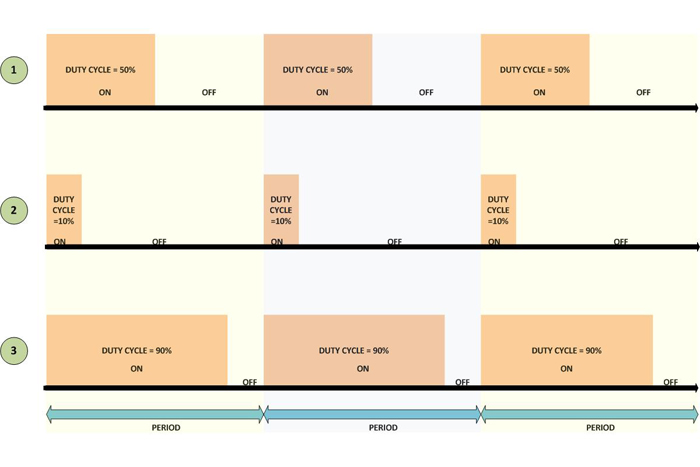
Fig. 2: PWM Waves Generated at P1A channel in PIC18F4550
The period of the wave is the sum of the ‘ON time + OFF time’. Duty-cycle is the percentage of time period for which the logic1 voltage exists in a cycle (ON time), starting from the beginning of the cycle.
The PWM is that kind of a wave in which the ON time and OFF time can vary in a cycle but the sum of ‘ON time + OFF time’ remains constant for every cycle.
Period = ON time + OFF time
Duty-cycle = ON time / (ON time + OFF time) = ON time / Period
Increasing the Duty-cycle will increase the voltage at the filter device’s output and decreasing the Duty-cycle will decrease the voltage as well.

Fig. 3: Voltage generated by PWM wave in interval between two interrupts
The voltage generated by the PWM wave in the interval between two interrupts will be a constant value and this time period can be called ‘sampling period’.
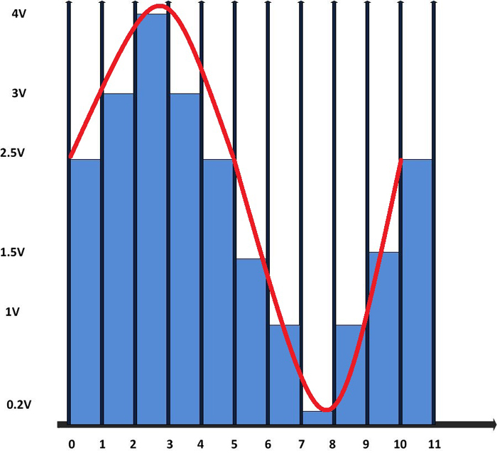
Fig. 4: Sample Values of CCPR1 register to generate PWM wave in PIC18F4550
The values that should be assigned to the CCPR1 register to generate such consecutive samples are actually taken from a look-up table. The look-up table with 50 samples which is used in this particular project to generate the sine wave is shown in the following;
|
Sample no. |
Value |
Sample no. |
Value |
Sample no. |
Value |
Sample no. |
Value |
Sample no. |
value |
|
1 |
52 |
11 |
85 |
21 |
69 |
31 |
28 |
41 |
16 |
|
2 |
57 |
12 |
86 |
22 |
65 |
32 |
25 |
42 |
18 |
|
3 |
62 |
13 |
86 |
23 |
61 |
33 |
22 |
43 |
20 |
|
4 |
66 |
14 |
86 |
24 |
56 |
34 |
19 |
44 |
23 |
|
5 |
70 |
15 |
85 |
25 |
52 |
35 |
17 |
45 |
26 |
|
6 |
74 |
16 |
83 |
26 |
48 |
36 |
15 |
46 |
39 |
|
7 |
77 |
17 |
81 |
27 |
44 |
37 |
14 |
47 |
34 |
|
8 |
80 |
18 |
78 |
28 |
39 |
38 |
14 |
48 |
38 |
|
9 |
82 |
19 |
75 |
29 |
35 |
39 |
14 |
49 |
43 |
|
10 |
84 |
20 |
72 |
30 |
31 |
40 |
15 |
50 |
48 |
Time period calculations:
In this section the calculations for the sampling time, PWM Period, PWM Duty-Cycle, frequency of the sine-wave etc. are calculated and the details of the calculations are available in a previous project on PIC Sine Wave Generation
Sampling time:
In this project the TMR0 is set to zero and the timer0 is configured as an 8 bit timer with pre-scale value 1:2 which gives a sampling time;
Sampling time = 40us
PWM period:
In this particular project the PR2 is written to a very small value so as to generate small time periods and hence to get more number of PWM cycles per sampling period.
PR2 = 22
The PWM Period = 2us
Number of PWM cycles per Sample = 20
Thus the timer0 will generate an interrupt after every 20 PWM cycles.
The frequency of the sine wave = 500 Hz
PWM Duty-cycle:
The Duty-cycle in this particular project is varied according to the look-up table whenever a timer0 interrupt occurs. The maximum Duty-cycle (100%) is 2us only since it is the value of the PWM period, hence
The CCPR1 can be written with any value between 0 and 100
The filter design:
The following figure shows a microcontroller generating PWM wave which is then used to generate the corresponding analog voltage with the help of a filter circuit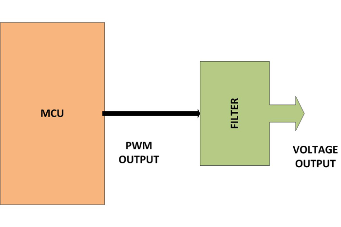
Fig. 5: Block Diagram of PIC microcontroller generating PWM wave
In this particular project the filter circuit is actually an integrator made with a single capacitor. The filter simply integrates the duty cycle of each PWM cycles and hence averages out the voltage in a PWM wave.The integrator is a circuit which has a resistor and a capacitor in series connected across the input and the ground and the analog voltage is obtained across the capacitor as shown in the following figure;

Fig. 6: Filter Circuit as integrator of PWM Cycle in Sound Generation using PIC
RC >= PWM Period
If the value for the C is taken as 0.1uF and the value of R is taken as 20 ohms, which will make an integrator circuit, required to generate the voltage equivalent of the PWM wave having a Period of 2us.
The driver circuit design:
The devices like LED can be directly driven by the PWM pin of the microcontroller, but when it comes to high power consuming devices like Loud Speaker or DC Motor etc. a specially designed driver circuit is necessary due to the following reasons.
The microcontroller is not able to source the required current
High current flow to the load attached to the PWM pin can cause internal drop of voltage inside the I/O pin and hence the PWM voltage level varies.
The filter circuit may not be able to generate the required voltage in such situations.
Making the microcontroller to source that much current may damage the microcontroller permanently.
In short the Load should get enough current and voltage without affecting the functioning of the filter circuit or the microcontroller.
The driver circuit itself consumes some current and hence the current flowing through the driver circuit from the PWM pin should also be limited. This can be done by connecting a high value series resistance with the driver circuit.
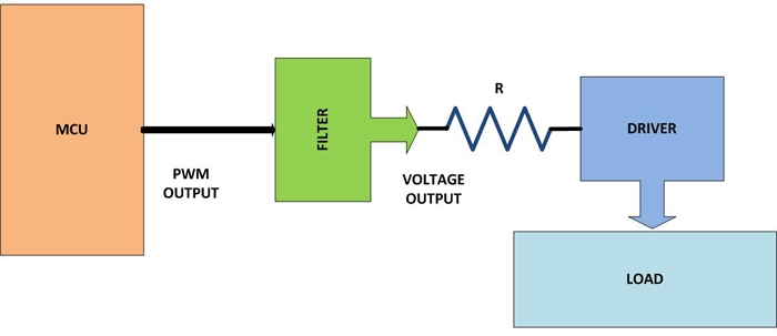
Fig. 7: Block Diagram of Sound Generation Ciruit using PIC
In this particular project the Darlington pair using two NPN transistors is used. The Darlington Pair can source very high current to the load device like relays, motors, loud speaker etc. however consuming very small amount of current from the input device. Hence this circuit is ideal for this kind of applications.
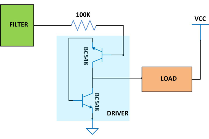
Fig. 8: Circuit Diagram Of NPN Transistor As Darlington Pair With An Input Current Limiting Resistor
The filter takes the PWM input from the microcontroller PWM pin and there it converts the modulated waveform to its equivalent voltage. In this particular project the output of the filter circuit is a sine wave. The sine wave is then send to the driver circuit consist of Darlington pair through a 100K resistor so as not to load the filter circuit by the driver. Now the driver source enough current to the loud speaker corresponding to the low current sine wave it is receiving.
The circuit:
The circuit operates on well regulated 5V supply with a 4MHz external crystal oscillator which forms 48MHz CPU clock with the help of an internal PLL. The standard 0.1uF capacitor is used as the filter circuit (RC integrator) to generate the voltage equivalent of the PWM. The capacitor is connected across the PWM pin (PIN 17) of the microcontroller and the ground. A Darlington pair is used to drive the loud speaker which can generate the sound equivalent of the sine wave frequency. The Darlington pair itself is connected to the filter circuit through a 100K resistor so as not to load the filter by the Darlington pair. The probe from the CRO can be connected across the ground and the PWM pin of the microcontroller incase if need to watch the sine wave.
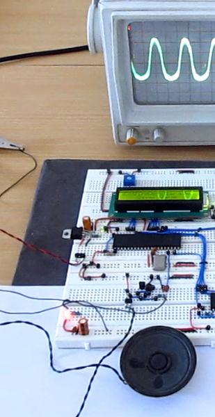
Fig. 9: Output Waveform of Audible sine wave by Loudspeaker on CRO
Tips for better results:
1. Always use a well regulated power supply, since very small ripples in the power supply can induce noise in the PWM wave generated by the microcontroller and hence affects their voltage generation at the filter circuit.
2. Use driver circuits as per the load requirement so as not to load or distort the PWM waveform
3.The period should not be less than which the load is not able to respond when using no filter circuits
4.The Duty-cycle should be select in such a way that it will generate the voltage in the range at which the load device can operate.
5. The filter circuit’s design should be precise so as to give maximum performance at the generated PWM Period and Duty-cycle.
6. Always operate the microcontroller at its maximum possible frequency so as to get maximum number of PWM cycles at any Sampling period, which will give a more stable voltage with the filter circuit or load.
7. Use more number of samples per sine wave (50 to 200 samples per sine wave cycle) to get better results
8. Use general purpose or audio frequency transistors having high current ratings for Darlington pair.
9.The loudness can be varied by varying the resistance which connects the filter circuit with the Darlington pair.
10. A variable resistor can be used as volume controller as decreasing the resistance will increase the volume and vice versa.
Project Source Code
### #include <p18f4550.h> #include <timers.h> //======================= chip config ===================// #pragma config PLLDIV = 1 #pragma config CPUDIV = OSC1_PLL2 #pragma config FOSC = HSPLL_HS #pragma config USBDIV = 1 #pragma config IESO = OFF #pragma config PWRT = OFF #pragma config BOR = OFF #pragma config VREGEN = OFF #pragma config WDT = OFF #pragma config WDTPS = 32768 #pragma config CCP2MX = ON #pragma config PBADEN = OFF #pragma config LPT1OSC = OFF #pragma config MCLRE = ON #pragma config STVREN = ON #pragma config LVP = OFF #pragma config ICPRT = OFF #pragma config XINST = OFF #pragma config DEBUG = OFF #pragma config WRTD = OFF //======================= chip config ===================// //LCD Control pins #define rs PORTBbits.RB4 #define rw PORTBbits.RB3 #define en PORTBbits.RB2 //LCD Data pins #define lcdport PORTD #define lcd_port_dir TRISD void lcd_clear ( void ); void lcd_2nd_line ( void ); void lcd_1st_line ( void ); void lcd_ini ( void ); void dis_cmd ( unsigned char cmd_value ); void dis_data ( unsigned char data_value ); void lcdcmd ( unsigned char cmdout ); void lcddata ( unsigned char dataout ); void delay_ms ( int delay ); //=============== SINE WAVE LOOK UP TABLE ================// const unsigned char sine[50] = { 52,57,62,66,70,74,77,80,82,84,85,86,86, 86,85,83,81,78,75,72,69,65,61,56,52, 48,44,39,35,31,28,25,22,19,17,15,14,14, 14,15,16,18,20,23,26,30,34,38,43,48 }; //=============== SINE WAVE LOOK UP TABLE ================// //============================ TIMER 0 ISR =================================// #pragma interrupt tmr0_interrupt void tmr0_interrupt(void) { static unsigned char i = 0; i ++; // method to write the sample values into the 10bit CCPR1 register // CCP1CON |= ( ( sine [ i ] ) << 5 ) & 0x03; CCPR1L = ( sine [ i ] ) >> 2; // method to write the sample values into the 10bit CCPR1 register // if ( i == 49 ) i = 0; else; INTCONbits.TMR0IF=0; // clearing the timer0 overflow bit } //============================ TIMER 0 ISR =================================// void main ( void ) { unsigned char data1 [] = "EngineersGarage"; unsigned char data2 [] = " Sine Wave "; int i = 0; OSCCON = 0x0C; lcd_ini (); // LCD initialization delay_ms ( 200 ); //========================= start up display on LCD ================================// while ( data1 [i] != '�' ) { dis_data ( data1 [i] ); delay_ms ( 200 ); i++; } i = 0; lcd_2nd_line (); while ( data2 [i] != '�' ) { dis_data ( data2 [i] ); delay_ms ( 200 ); i++; } i = 0; /========================= start up display on LCD ================================// //============================ PWM SETTINGS ====================================// TMR2 = 0x0 // setting TMR2 value as 0, start counting from 0 PR2 = 22; // set the PR2 value, to get PWM period of 2us CCPR1L = 0x00; // setting initial value of CCPR1L as 0 CCP1CON = 0x0C; // select single output with P1A, and mode select bits so as to get P1A, P1B, P1C and // P1D as active-high TRISC &= 0xFB; // setting the PWM pin as output T2CON = 0x04; // both the pre-scalar and post-scalar bits are written for 1:1 with the timer2 turned on. INTCONbits.T0IF = 0; // turning off the Timer0 interrupt TMR0L = 0xFE; // setting the timer register to value T0CON = 0xC0; // enable the timer, select the timer in 8bit, select CLKO, assign the pre-scale value 1:4 INTCONbits.TMR0IF=0; // clearing the timer0 overflow bit INTCONbits.T0IE = 1; // enabling the timer0 interrupt INTCONbits.GIE =1; // enabling the global interrupts //============================ PWM SETTINGS ====================================// while ( 1 ) { ; } } //======================== LCD routines defenitions ========================// void delay_ms ( int delay ) { int ms, i; for ( ms = 0; ms < delay; ms ++ ) for ( i = 0; i < 70; i ++ ); } void lcd_ini ( void ) { TRISB &= 0xE3; lcd_port_dir &= 0x0F; dis_cmd ( 0x02 ); // to initialize LCD in 4-bit mode. dis_cmd ( 0x28 ); //to initialize LCD in 2 lines, 5X7 dots and 4bit mode. dis_cmd ( 0x0C ); dis_cmd ( 0x06 ); dis_cmd ( 0x80 ); dis_cmd ( 0x01 ); delay_ms ( 500 ); } void dis_cmd ( unsigned char cmd_value ) { unsigned char cmd_value1; cmd_value1 = cmd_value & 0xF0; //mask lower nibble because PA4-PA7 pins are used. lcdcmd ( cmd_value1 ); // send to LCD cmd_value1 = ( ( cmd_value << 4 ) & 0xF0 ); //shift 4-bit and mask lcdcmd ( cmd_value1 ); // send to LCD } void dis_data ( unsigned char data_value ) { unsigned char data_value1; data_value1 = data_value & 0xF0; lcddata ( data_value1 ); data_value1 = ( ( data_value << 4 ) & 0xF0 ); lcddata ( data_value1 ); } void lcdcmd ( unsigned char cmdout ) { lcdport &= 0x0F; lcdport |= cmdout; rs = 0; rw = 0; en = 1; delay_ms ( 50 ); en = 0; delay_ms ( 50 ); } void lcddata ( unsigned char dataout ) { lcdport &= 0x0F; lcdport |= dataout; rs = 1; rw = 0; en = 1; delay_ms ( 50 ); en = 0; delay_ms ( 50 ); } void lcd_clear(void) { dis_cmd(0x01); delay_ms(10); } void lcd_2nd_line(void) { dis_cmd(0xC0); delay_ms(1); } void lcd_1st_line(void) { dis_cmd(0x80); delay_ms(1); } //======================== LCD routines defenitions ========================// ###
Project Components
Project Video
Filed Under: PIC Microcontroller.
Filed Under: PIC Microcontroller.


Questions related to this article?
👉Ask and discuss on EDAboard.com and Electro-Tech-Online.com forums.
Tell Us What You Think!!
You must be logged in to post a comment.