Pulse Width Modulation (PWM) is a technique in which the width of a pulse is modulated keeping the time period of the wave constant. One cycle has a fixed time period called ‘Period’ and a varying on time called ‘Duty cycle’. The entire wave can have two voltages levels either logic 0 or logic 1.
The PIC18F4550 has an inbuilt PWM module which can generate continuous PWM waves. The Period and the duty cycle of the PWMwave can be adjusted in program. This project explores the PWM module of the PIC18F4550 and tries to glow an LED with varying intensities, which shows that it is possible to generate any required voltage at a pin of a digital microcontroller with the help of PWM waves.
PWM is a digital wave that can be generated using digital circuits which are not capable of generating analog voltages. With the help of the modulation of the width of a pulse in a period of the wave, they can generate any required voltage with the help of a proper filter circuits. Thus the PWM wave is always associated with a filter circuit which has been designed according to the timing details of the pulse.
The following figure shows a microcontroller generating PWM wave which is then used to generate the corresponding analog voltage with the help of a filter circuit.

Fig. 2: Block Diagram of PIC Micro-controller generating PWM wave with filer Circuit
The filter could be any device which can generate the equivalent voltage of a PWM voltage. It normally consists of Low-pass filters, amplifiers, load drivers etc. They generate the voltage and fed that voltage to the load device. In certain cases where the load itself can act as a filter generating the voltage from the PWM wave and drive itself using that voltage. The example of such a devices which can itself act as a PWM filter is DC motor. In this particular project also there is no filter circuit since the aim is to vary the intensity of a glowing LED only. It doesn’t mean that the LED can act as a filter; rather it is the persistence of vision that makes one feel that the intensity of the LED is varying. In this case the LED is glowing normally for the logic1 and logic0 voltages of a PWM, but the variation in the ON time make one feel that the intensity is varying. Here the persistence of vision plays the key role and the filter device is nothing but our eyes itself.
The PIC18F4550 has four PWM output channels and they are P1A, P1B, P1C and P1D. All of them are capable of generating PWM waves at a time. In this project only one of the PWM channels are using. The P1A is the PWM channel in this particular project. A simple example of the of waves generated at this pin is shown below;

Fig. 3: Output PWM Wave at PA1 in PIC18F4550 Microcontroller to Glow LED
As shown in the above figure the ‘Period’ of all the wave remains the same but their ‘Duty-cycle’ varies.
The period of the wave is the sum of the ‘ON time + OFF time’. Duty-cycle is the percentage of time period for which the logic1 voltage exists in a cycle (ON time), starting from the beginning of the cycle.
The PWM is that kind of a wave in which the ON time and OFF time can vary in a cycle but the sum of ‘ON time + OFF time’ remains constant for every cycle.
The period and the duty cycle for a PWM wave can be calculated generally using the following equations;
Period = ON time + OFF time
Duty-cycle = ON time / (ON time + OFF time) = ON time / Period
As shown in the figure, the first PWM wave has a Duty-cycle of 50% which means the on-time is exactly half of that the period of the wave. The second wave has 10% Duty-cycleand the third wave has 90% Duty-cycle. When applied to a proper filter the 50% duty cycle can produce half of the maximum voltage of the pulse. If the maximum voltage (logic 1 voltage) of the pulse is 5V then the 50% duty cycle wave can produce a continuous 2.5V. The 10% duty cycle wave can produce nearly 0 voltages and the 90% duty cycle wave can produce nearly 5V.Thus the wave when applied to a filter can continuously produce a voltage which is the average of the voltage in a single period.
Increasing the Duty-cycle will increase the voltage at the filter device’s output and decreasing the Duty-cycle will decrease the voltage as well
The filter could be anything like a capacitor or inductor. Even though if there is no filter most of the device can generate a corresponding output with a PWM wave resembles that the device is operating at the average voltage of that PWM wave. The LED in this project is the simplest example for such a kind of device.
The registers:
The registers which help in generating the Period and the Duty cycle of the PWM module in a PIC18F4550 are CPR1, PR2 and TMR2. The TMR2 and the PR2 are the timer value and the Pre-scalar value registers of the Timer2 module. They are used to generate the Period of the PWM wave. The CCPR1 is a 10 bit register which can be used to set the duty cycle of the PWM wave.
Suppose one have written the required values into the PR2 and the CCPR1 registers for the Period and Duty cycle of the PWM wave. The TMR2 value is always set to zero once the PWM module is enabled. Once the module is enabled then with each clock the timer2 receives, the value in the TMR2 increases. Hence these registers act like up-counters. This value in the TMR2 register is always under a comparison with the values in the PR2 register and the CCPR1 register like as shown in the following figure;

Fig. 4: Block Diagram of Registers to set time and duty cycle of PWM module in PIC
As per the above figure, the Duty-cycle (on-time) is available until the TMR2 value exceeds the CCPR1 value, since the Duty-cycle is the output of the comparator which compares the TMR2 value with the CCPR1 value. The Period of the wave is available further until the value in the TMR2 exceeds the PR2 value since the Period is the output of the comparator which compares the TMR2 value with the PR2 value
Once the value in the TMR2 exceeds that of the PR2 then the TMR2 is cleared to zero and starts counting again. Hence continuous PWM wave with specified duty cycle and Period is available at the PWM output pin. Once can rewrite the CCPR1 value any time to change the duty cycle of the PWM wave so as to change the voltage which the wave is generating at the filter device connected to the PWM pin of the microcontroller.
The Period of the PWM wave in PIC18F4550 given by;
PWM Period = [(PR2) + 1] * 4 * TOSC * (TMR2 Pre-scale Value)
The Duty cycle of the PWM wave in PIC18F4550 is given by;
PWM Duty Cycle = (CCPR1 * TOSC * (TMR2 Pre-scale Value)
CCP1CON
This is the register which controls the PWM operation in PIC18F4550. It can be used to configure the PWM output channels and enable the PWM module in the required mode and can also be used to set the lower two bits of the duty cycle value.
{C}{C}{C}{C}{C}{C}{C}{C}{C}{C}{C}{C}{C}{C}
{C}{C}{C}{C}{C}{C}{C}{C}{C}{C}{C}{C}{C}{C}
|
Output Configuration bits |
Duty Cycle Bit 1 |
Duty Cycle Bit 0 |
Mode Select bits |
||||
|
7 |
6 |
5 |
4 |
3 |
2 |
1 |
0 |
Fig. 5: CCP1CON Register in PIC
The output configuration bits can be written to select the ‘single-output’, ‘full bridge’, ‘half bridge ‘or ‘full-bridge’ output reverse modes with the four PWM channels. This particular project uses the single-output PWM at P1A channel.
The output configuration can be done as shown in the following table;
|
Output Configuration bits |
Description |
|
|
P1M1 |
P1M0 |
|
|
0 |
0 |
Single output: P1A modulated; P1B, P1C, P1D assigned as port pins |
|
0 |
1 |
Full-bridge output forward: P1D modulated; P1A active; P1B, P1C inactive |
|
1 |
0 |
Half-bridge output: P1A, P1B modulated with dead-band control; P1C, P1D assigned as port pins |
|
1 |
1 |
Full-bridge output reverse: P1B modulated; P1C active; P1A, P1D inactive |
Fig. 6: Mode Select bits for PWM Output channels in PIC
Duty cycle bit 1 and Duty cycle bit 0 are the two lower bits of the CPR1 register which can be used to set the duty cycle of the PWM waveform.
The Mode select bits can be used to select the modes of the PWM of the four PWM output channels. The four possible output modes are shown in the following table;
|
Mode Select bits |
Description |
|||
|
CCP1M3 |
CCP1M2 |
CCP1M1 |
CCP1M0 |
|
|
1 |
1 |
0 |
0 |
P1A, P1C Active-High; P1B, P1D active-high |
|
1 |
1 |
0 |
1 |
P1A, P1C Active-High; P1B, P1D active-low |
|
1 |
1 |
1 |
0 |
P1A, P1C Active-Low; P1B, P1D active-high |
|
1 |
1 |
1 |
1 |
P1A, P1C Active-Low; P1B, P1D active-low |
Fig. 7: Output Configuration bit at P1A channel to glow LED.
In this project the output configuration bits are selected so as to select single output with P1A, and mode select bits so as to get P1A, P1B, P1C and P1D as active-high, which means they will be high during the duty cycle.
Hence the value of the CCP1CON register can be written as;
CCP1CON = 0x0C
T2CON
This register of the timer2 module can be written to set the timer pre-scalar and post-scalars and also to turn on/off the timer2.
{C}{C}{C}{C}{C}{C}{C}{C}{C}{C}{C}{C}{C}{C}
{C}{C}{C}{C}{C}{C}{C}{C}{C}{C}{C}{C}{C}{C}
|
Unimplemented |
Post-scale Select bits |
Timer2 On bit |
Pre-scale Select bits |
|||||
|
0 |
1 |
2 |
3 |
4 |
5 |
6 |
7 |
|
Fig. 8: Bit Configuration of T2CON Register in PIC
The MSB is unimplemented. The following four bits can be used to set the post-scalar as shown below;
|
Post-scale Select bits |
Description |
|||
|
T2OUTPS3 |
T2OUTPS2 |
T2OUTPS1 |
T2OUTPS0 |
|
|
0 |
0 |
0 |
0 |
1:1 Post-scale |
|
0 |
0 |
0 |
1 |
1:2 Post-scale |
|
0 |
0 |
1 |
0 |
1:3 Post-scale |
|
0 |
0 |
1 |
1 |
1:4 Post-scale |
|
0 |
1 |
0 |
0 |
1:5 Post-scale |
|
0 |
1 |
0 |
1 |
1:6 Post-scale |
|
0 |
1 |
1 |
0 |
1:7 Post-scale |
|
0 |
1 |
1 |
1 |
1:8 Post-scale |
|
1 |
0 |
0 |
0 |
1:9 Post-scale |
|
1 |
0 |
0 |
1 |
1:10 Post-scale |
|
1 |
0 |
1 |
0 |
1:11 Post-scale |
|
1 |
0 |
1 |
1 |
1:12 Post-scale |
|
1 |
1 |
0 |
0 |
1:13 Post-scale |
|
1 |
1 |
0 |
1 |
1:14 Post-scale |
|
1 |
1 |
1 |
0 |
1:15 Post-scale |
|
1 |
1 |
1 |
1 |
1:16 Post-scale |
Fig. 9: Bit Combination of Timers to set post-scalar Values in PIC
Timer2 ON bit can be used to turn ON/OFF the timer2 module.
|
Timer2 On bit |
Description |
|
TMR2ON |
|
|
0 |
OFF the timer |
|
1 |
ON the timer |
Fig. 10: Bit Value for Timer2 ON in LED Glowing Circuit
The two LSB bits can be written to set the Pre-scalar as shown in the following table;
|
Pre-scale Select bits |
Description |
|
|
T2CKPS1 |
T2CKPS0 |
|
|
0 |
0 |
Pre-scalar is 1 |
|
0 |
1 |
Pre-scalar is 4 |
|
1 |
x |
Pre-scalar is 16 |
Fig. 11: Pre-Scalor Bit Values for Timer
In this project both the pre-scalar and post-scalar bits are written for 1:1 with the timer2 turned on. Hence the value that can be written into the T2CON is;
T2CON = 0x04
The voltage generated by the PWM wave at a filter device can vary by simply varying the Duty-cycle of the PWM wave. Increasing the Duty-cycle will increase the voltage at the filter device’s output and decreasing the Duty-cycle will decrease the voltage as well. In this particular project the brightness of the LED is varied by periodically re-writing the value of the CCPR1 register to vary the Duty-cycle. It is done by generating interrupts periodically with another timer module timer0 and changing the CCPR1 value when the code is inside the timer0’s ISR. It is done as shown in the following figure;

Fig. 12: Voltage generated by PWM wave after varying register value in PIC
The voltage generated by the PWM wave in the interval between two interrupts will be a constant value and this time period can be called Sampling time.
A sampling time can have 10 to 500 PWM cycles normally and depends on the particular output device requirement.
The more the number of PWM cycles in a Sampling time, more stable the output voltage will be
The Duty-cycle of the PWM wave is increased slightly each times the timer0 fires and to perform such a thing one has to configure the timer0 properly. The following section explains how to set the timer0 for this particular project.
The timer0 can be set in 8 bit and 16 bit mode with or without pre-scalar assigned into it. The important register associated with the timer0 module is T0CON, TMR0H and TMR0L registers. The T0CON register controls the timer0 module and the TMR0H and TMR0L registers together act as the 16 bit timer0 register.
T0CON
The T0CON is the timer0 control register which can be written to turn ON/OFF the timer0, select 8/16 bit of operation, select the clock, select the clock edge, select and assign the pre-scalar.
|
On/Off Control bit |
8-Bit/16-Bit Control bit |
Clock Source Select bit |
Source Edge Select bit |
Pre-scalar Assignment bit |
Pre-scalar Select bits |
||
|
7 |
6 |
5 |
4 |
3 |
2 |
1 |
0 |
The On/Off Control bit can be used to turn on or off the timer0 module.
|
On/Off Control bit |
Description |
|
TMR0ON |
|
|
0 |
OFF the timer |
|
1 |
ON the timer |
The 8-Bit/16-Bit Control bit can be written to select the 16 bit or 8 bit operation of the timer0.
|
8-Bit/16-Bit Control bit |
Description |
|
T08BIT |
|
|
0 |
Timer0 is configured as a 16-bit timer/counter |
|
1 |
Timer0 is configured as an 8-bit timer/counter |
The fifth bit which is the Clock Source Select bit can be written to select the internal instruction cycle clock or the external clock obtained at the T0CKI pin.
|
Clock Source Select bit |
Description |
|
T0CS |
|
|
0 |
Internal instruction cycle clock (CLKO) |
|
1 |
Transition on T0CKI pin |
The Source Edge Select bit can be written to select the clock edge on which the value in the timer0 register should increment if one selects the clock from the T0CKI pin.
|
Source Edge Select bit |
Description |
|
T0SE |
|
|
0 |
Increment on low-to-high transition on T0CKI pin |
|
1 |
Increment on high-to-low transition on T0CKI pin |
The Pre-scalar Assignment bit can be used to assign or not to assign the pre-scalar with the timer0 module.
|
Pre-scalar Assignment bit |
Description |
|
PSA |
|
|
0 |
Timer0 pre-scalar is assigned |
|
1 |
Timer0 pre-scalar is NOT assigned |
The last three bits in the LSB side can be used to select the pre-scalar for the timer0. Depending on the bit combinations eight different pre-scalars can be selected as shown in the following table;
|
Pre-scalar Select bits |
Description |
||
|
T0PS2 |
T0PS1 |
T0PS0 |
|
|
1 |
1 |
1 |
1:256 Pre-scale value |
|
1 |
1 |
0 |
1:128 Pre-scale value |
|
1 |
0 |
1 |
1:64 Pre-scale value |
|
1 |
0 |
0 |
1:32 Pre-scale value |
|
0 |
1 |
1 |
1:16 Pre-scale value |
|
0 |
1 |
0 |
1:8 Pre-scale value |
|
0 |
0 |
1 |
1:4 Pre-scale value |
|
0 |
0 |
0 |
1:2 Pre-scale value |
In this particular project the value to the T0CON is written so as to enable the timer, select the timer in 8 bit mode, select CLKO, and assign the pre-scale value 1:4. The corresponding value is given as;
T0CON = 0x81
Time period calculations:
Sampling time:
In this project the TMR0 is set to zero and the timer0 is configured as a 16 bit timer. Now the timer will count from 0x0000 to 0xFFFF with a clock frequency of FOSC/4 and a pre-scale of 1:4.
The CPU clock frequency is set as 48MHz and hence the time period of a single clock TOSC can be calculated as
TOSC = 1/ FOSC =(1 / (48*10^-6) = 0.02 * 10^-6seconds.
The time period of the clock which the timer0 module receives can be calculated as
1 / (FOSC/4) = TOSC * 4 = (0.02 * 10^-6) * 4 = 0.08 * 10^-6 seconds.
The timer0 has a pre-scale value of 1:4 and hence the time period should be again multiplied by 4.
Hence the time period at which the value in the 16 bit timer increases = (0.08 * 10^-6) * 4 = 0.32*10^-6 seconds.
The timer0 value increases from 0x0000 to 0xFFFF with a time period of 0.32*10^-6 seconds.
0.32 * 10^-6 * 65535 which gives a value almost equal to 20ms.
The Sampling time = 20ms
PWM period:
In this particular project the PR2 is written to its maximum possible value so as to get the maximum Period.
PR2 = 0xFF
Using the equation for calculating the Period of the PWM wave given as;
PWM Period = [(PR2) + 1] * 4 * TOSC * (TMR2 Pre-scale Value)
The TMR2 Pre-scalar value is selected as 1 and the TOSC is already calculated as 0.02 * 10^-6 seconds.
PWM period = [255 + 1] * 4 * (0.02 * 10^-6) * 1
This can give a value almost equal to 0.02ms.
The PWM Period = 0.02ms
Thus in a Sampling time number of PWM cycles can be calculated as 20 / 0.02 = 1000 PWM cycles.
Number of PWM cycles per Sample = 1000
This much number of PWM cycles per sample is good enough to generate a stable output voltage in a filter device.
PWM Duty-cycle:
The Duty-cycle in this particular project is varied whenever a timer0 interrupt occurs. The maximum Duty-cycle (100%) is 0.02ms only since it is the value of the PWM period. The Duty-cycle generated by the microcontroller depends on the value in CCPR1 register and for a maximum value of 0.02ms the value that should be written in the CCPR1 register can be calculated using the equation for PWM Duty-cycle;
PWM Duty Cycle = (CCPR1 * TOSC * (TMR2 Pre-scale Value)
Using the above equation,
The value of CCPR1 = PWM duty cycle / (TOSC * (TMR2 Pre-scale Value))
The TMR2 Pre-scalar value is selected as 1 and the TOSC is already calculated as 0.02 * 10^-6 seconds.
CCPR1 = 0.02 * 10^-3 / 0.02 * 10^-6 = 1000
The CCPR1 can be written with any value between 0 and 1000 toget a corresponding Duty-cycle
The Duty-cycle should be select in such a way that it will generate the voltage in the range at which the load device can operate. It was found experimentally that the value between 30 and 70 can generate visible intensity variations with a 5mm Red LED. So in this project the CCPR1 is written with values between 30 and 70 only.
The circuit:
In this particular project an LED is connected to the PWM channel of the PIC18F4550 microcontroller through a current-limiting resistor. There is no filter circuit in this project since the persistence of vision of the human eye can generate the sensation of varying intensity.The circuit operates on a 4MHz external crystal oscillator which forms 48MHz CPU clock with the help of an internal PLL.
Tips for better results:
{C}{C}{C}{C}{C}{C}{C}{C}{C}{C}{C}{C}{C}{C}· 11.{C}{C}{C}{C}{C}{C}{C}{C}{C}{C}{C}{C}{C}{C}Always use a well regulated power supply, since very small ripples in the power supply can induce noise in the PWM wave generated by the microcontroller and hence affects their voltage generation at the filter circuit.
{C}{C}{C}{C}{C}{C}{C}{C}{C}{C}{C}{C}{C}{C}· 2.{C}{C}{C}{C}{C}{C}{C}{C}{C}{C}{C}{C}{C}{C}Use driver circuits as per the load requirement so as not to load or distort the PWM waveform
{C}{C}{C}{C}{C}{C}{C}{C}{C}{C}{C}{C}{C}{C}· 3.{C}{C}{C}{C}{C}{C}{C}{C}{C}{C}{C}{C}{C}{C}The period should not be less than which the load is not able to respond when using no filter circuits
{C}{C}{C}{C}{C}{C}{C}{C}{C}{C}{C}{C}{C}{C}· 4.{C}{C}{C}{C}{C}{C}{C}{C}{C}{C}{C}{C}{C}{C}The Duty-cycle should be select in such a way that it will generate the voltage in the range at which the load device can operate.
{C}{C}{C}{C}{C}{C}{C}{C}{C}{C}{C}{C}{C}{C}· 5.{C}{C}{C}{C}{C}{C}{C}{C}{C}{C}{C}{C}{C}{C}The filter circuit’s design should be precise so as to give maximum performance at the generated PWM Period and Duty-cycle.
{C}{C}{C}{C}{C}{C}{C}{C}{C}{C}{C}{C}{C}{C}· 6.{C}{C}{C}{C}{C}{C}{C}{C}{C}{C}{C}{C}{C}{C}Always operate the microcontroller at its maximum possible frequency so as to get maximum number of PWM cycles at any Sampling period, which will give a more stable voltage with the filter circuit or load.
Project Source Code
###
#include <p18f4550.h>#include <timers.h>//======================= chip config ===================//#pragma config PLLDIV = 1#pragma config CPUDIV = OSC1_PLL2#pragma config FOSC = HSPLL_HS#pragma config USBDIV = 1#pragma config IESO = OFF#pragma config PWRT = OFF#pragma config BOR = OFF#pragma config VREGEN = OFF#pragma config WDT = OFF#pragma config WDTPS = 32768#pragma config CCP2MX = ON#pragma config PBADEN = OFF#pragma config LPT1OSC = OFF#pragma config MCLRE = ON#pragma config STVREN = ON#pragma config LVP = OFF#pragma config ICPRT = OFF#pragma config XINST = OFF#pragma config DEBUG = OFF#pragma config WRTD = OFF//======================= chip config ===================////LCD Control pins#define rs PORTBbits.RB4#define rw PORTBbits.RB3#define en PORTBbits.RB2//LCD Data pins#define lcdport PORTD#define lcd_port_dir TRISDvoid lcd_clear ( void );void lcd_2nd_line ( void );void lcd_1st_line ( void );void lcd_ini ( void );void dis_cmd ( unsigned char cmd_value );void dis_data ( unsigned char data_value );void lcdcmd ( unsigned char cmdout );void lcddata ( unsigned char dataout );void delay_ms ( int delay );//============================ TIMER 0 ISR =================================//#pragma interrupt tmr0_interruptvoid tmr0_interrupt(void){static unsigned char i = 30;static int count_up_down = 1;if ( count_up_down ){i ++;// method to write the value of 'i' into the 10bit CCPR1 register //CCP1CON |= ( i << 5 ) & 0x03;CCPR1L = i >> 2;// method to write the value of 'i' into the 10bit CCPR1 register //if ( i == 70 )count_up_down = 0;else;}else{i --;CCP1CON |= ( i << 5 ) & 0x03;CCPR1L = i >> 2;if ( i == 30 )count_up_down = 1;else;}INTCONbits.TMR0IF=0; // clearing the timer0 overflow bit}//============================ TIMER 0 ISR =================================//void main ( void ){unsigned char data1 [] = "EngineersGarage";unsigned char data2 [] = " PWM demo ";int i = 0;OSCCON = 0x0C; // set CPU Frequency as 8 MHzlcd_ini (); // LCD initializationdelay_ms ( 200 );//========================= start up display on LCD ================================//while ( data1 [i] != '�' ){dis_data ( data1 [i] );delay_ms ( 200 );i++;}i = 0;lcd_2nd_line ();while ( data2 [i] != '�' ){dis_data ( data2 [i] );delay_ms ( 200 );i++;}i = 0;//========================= start up display on LCD ================================////============================ PWM SETTINGS ====================================//TMR2 = 0x00; // setting TMR2 value as 0, start counting from 0PR2 = 0xFF; // set the maximum PR2 value, to get PWM period of 0.02msCCPR1L = 0x00; // setting initial value of CCPR1L as 0CCP1CON = 0x0C; // select single output with P1A, and mode select bits so as to get P1A,P1B, P1C and // P1D as active-highTRISC &= 0xFB; // setting the PWM pin as outputT2CON = 0x04; // both the pre-scalar and post-scalar bits are written for 1:1 withthe timer2 turned on.INTCONbits.T0IF = 0; // turning off the Timer0 interruptTMR0H = 0x00; // setting the timer register to 0 so as to get maximum count,20ms time delayTMR0L = 0x00;T0CON = 0x81; // enable the timer, select the timer in 16, select CLKO, assign thepre-scale value 1:4INTCONbits.TMR0IF=0; // clearing the timer0 overflow bitINTCONbits.T0IE = 1; // enabling the timer0 interruptINTCONbits.GIE = 1; // enabling the global interrupts//============================ PWM SETTINGS ====================================//while ( 1 ){;}}//======================== LCD routines defenitions ========================//void delay_ms ( int delay ){int ms, i;for ( ms = 0; ms < delay; ms ++ )for ( i = 0; i < 70; i ++ );}void lcd_ini ( void ){TRISB &= 0xE3;lcd_port_dir &= 0x0F;dis_cmd ( 0x02 ); // to initialize LCD in 4-bit mode.dis_cmd ( 0x28 ); //to initialize LCD in 2 lines, 5X7 dots and 4bit mode.dis_cmd ( 0x0C );dis_cmd ( 0x06 );dis_cmd ( 0x80 );dis_cmd ( 0x01 );delay_ms ( 500 );}void dis_cmd ( unsigned char cmd_value ){unsigned char cmd_value1;cmd_value1 = cmd_value & 0xF0; //mask lower nibble because PA4-PA7 pins are used.lcdcmd ( cmd_value1 ); // send to LCDcmd_value1 = ( ( cmd_value << 4 ) & 0xF0 ); //shift 4-bit and masklcdcmd ( cmd_value1 ); // send to LCD}void dis_data ( unsigned char data_value ){unsigned char data_value1;data_value1 = data_value & 0xF0;lcddata ( data_value1 );data_value1 = ( ( data_value << 4 ) & 0xF0 );lcddata ( data_value1 );}void lcdcmd ( unsigned char cmdout ){lcdport &= 0x0F;lcdport |= cmdout;rs = 0;rw = 0;en = 1;delay_ms ( 50 );en = 0;delay_ms ( 50 );}void lcddata ( unsigned char dataout ){lcdport &= 0x0F;lcdport |= dataout;rs = 1;rw = 0;en = 1;delay_ms ( 50 );en = 0;delay_ms ( 50 );}void lcd_clear(void){dis_cmd(0x01);delay_ms(10);}void lcd_2nd_line(void){dis_cmd(0xC0);delay_ms(1);}void lcd_1st_line(void){dis_cmd(0x80);delay_ms(1);}//======================== LCD routines defenitions ========================//###
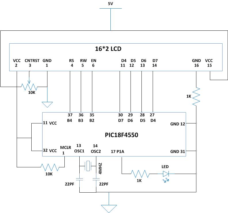
Circuit Diagrams
Project Components
Project Video
Filed Under: PIC Microcontroller.
Filed Under: PIC Microcontroller.

Questions related to this article?
👉Ask and discuss on Electro-Tech-Online.com and EDAboard.com forums.
Tell Us What You Think!!
You must be logged in to post a comment.