USB Flash Drives or commonly called as Pen Drives are popular removable storage media having a storage capacity up to 256 GB. They are preferred over the other conventional storage devices like floppy disks or CD ROMs as they are faster, smaller and have a longer life span.
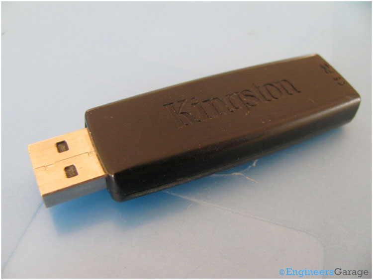
Fig. 1: Image of a 4-GB Pen Drive
The internal circuitry of the pen drive draws power from the computer for its operation. They have an integrated USB interface to communicate with the computer. The important parts of the pen drive are USB connector, crystal oscillator, memory chips and a controller to interact with the PC. The pen drive used here has storage capacity of 4GB.
Internal Structure
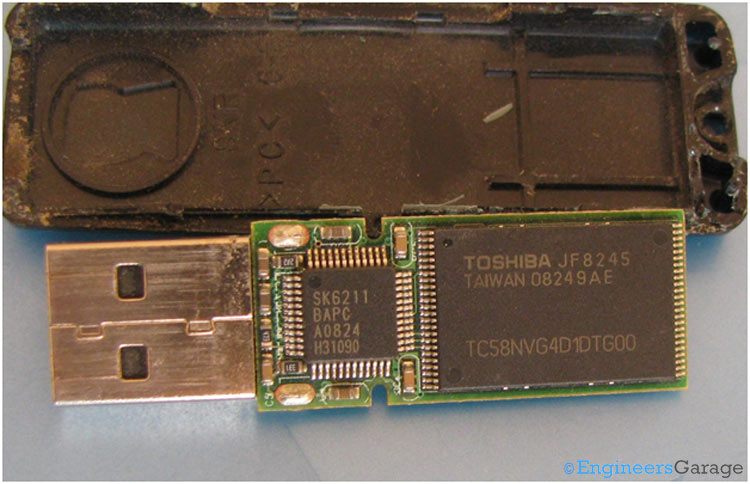
Fig. 2: Internal Structure of USB Showing PCB and Circuit Elements
A printed circuit board carrying the circuit elements and a USB connector is shown in the above image. The circuitry is protected inside a pair of plastic cases (connected to each other by means of mechanical hooks) which can be carried in a pocket or a key chain. The USB connector is protected by either retracting into the body or by covering by a removable lid. There are two chips, one is the USB controller and the other is the flash memory chip, which are discussed in detail later in the article.
Controller

Fig. 3: IC SK6211 Controller
The IC SK6211 shown in the above image is a controller which facilitates the data communication between the PC/Laptop and the flash memory (EEPROM) of the pen drive. It is fully compatible with USB 2.0 protocols and USB Mass storage class V1.0 specification. The devices like memory card, hard disk, pen drive etc with high data storage capacity fall under the category of Mass Storage Devices. In order to communicate data with devices falling under this category the USB has defined a set of protocols. The operating system provides inbuilt libraries to handle such devices thereby preventing the need of any external drivers to be installed before using these devices. This controller IC can interface with all kind of NAND EEPROM.
Memory Chip-1
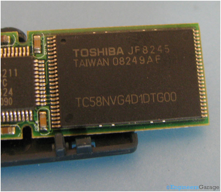
Fig. 4: NAND-type Flash Memory Chip
The second chip which is shown in the image above is a NAND type flash memory which has fast read, write and erase cycles. The data is stored in memory cells of the EEPROM, known as “floating gate transistors” – a regular metal-oxide field effect transistor (M0SFET) consisting three terminals – source, gate and drain. The storage capacity of this memory is 2GB. There is another similar chip with storage capacity of 2GB on the other side of the PCB, thereby making the total capacity of the pen drive to be 4GB.
Memory Chip-2 & Oscillator
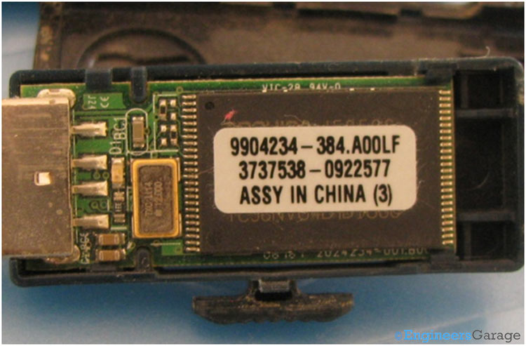
Fig. 5: Memory Chip of PCB and Various Components
The above image shows the other side of PCB. The second memory chip, a crystal oscillator and a number of surface mount components are soldered which are required for the operation of the pen drive.
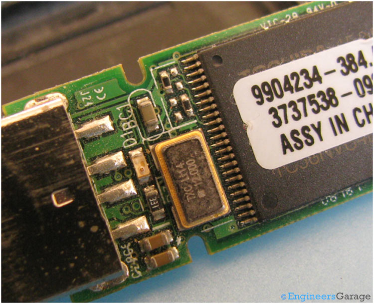
Fig. 6: Closer View of Circuit Board
The crystal oscillator produces the clock signal for the correct operation of the device. The crystal oscillator used here runs at a clock frequency at 12 MHz.
Filed Under: Insight


Questions related to this article?
👉Ask and discuss on Electro-Tech-Online.com and EDAboard.com forums.
Tell Us What You Think!!
You must be logged in to post a comment.