The modern world is filled with gadgets that get excited when they sense human motion. Automatic doors in elevators and shopping malls, burglar alarms at houses and shops, automatic lighting systems, electronic amenities in washrooms are just a few examples where human presence or absence puts the device into active or passive state. Smart, right? Now, what if we tell you that behind this smart response to motion is a gizmo that does not even reach the 2cm mark in size. Known as Pyroelectric or Passive Infrared Sensor (PIR, in both cases), this small electronic device is the curious case for this Insight.
Every object that has a temperature above perfect zero emits thermal energy (heat) in form of radiation. We, Homo sapiens, radiate at wavelength of 9-10micrometers all time of the day. The PIR sensors are tuned to detect this IR wavelength which only emanates when a human being arrives in their proximity. The term “pyroelectricity” means: heat that generates electricity (here, an electric signal of small amplitude). Since these sensors do not have an infrared source of their own, they are also termed as passive.
How does PIR sensor selectively responds to human radiated IRs? Upto what range can this sensor work? What lies inside this sensor that makes it work? This and answers to more questions in this Insight on PIR sensors. What adds more charm to this Insight is that the Panasonic 10m sensor taken is also one of the smallest PIR sensors commercially available till date.
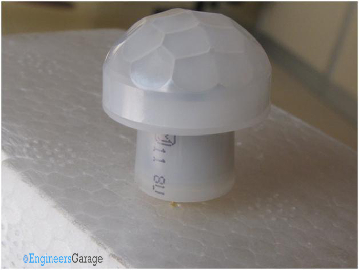
Fig. 1: Image of Panasonic 10-mm IR Sensor
Fresnel Lens Array
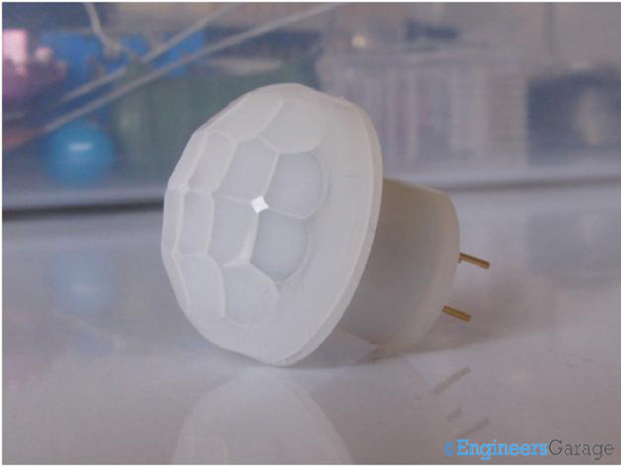
Fig. 2: Image of Sensor Outer Body
Image 02 shows a Panasonic 10m sensor: the PIR sensor unit enclosed in a plastic chamber. The chamber is translucent, donned with a beehive like cap and has an opening at the bottom from which the solder dip legs of the sensor protrude.
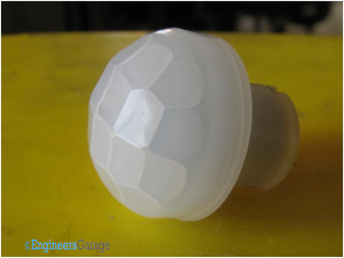
Fig. 3: Image showing the Beehive Structure and Curved Segments of Top Region of Sensor
On closely observing the top region of the sensor, the beehive structure, curved segments are seen. These curved segments are Fresnel lenses which constitute an array that increases the detection zone of the sensor. Fresnel lens array is known to capture more infrared radiation and focus it to a relatively smaller point. Detection is more stable and maximum distance for detection is also increased. Fresnel lens has been crafted to be translucent so that it can capture only infrared radiation without getting unwanted radiations from visible spectrum of light.
The number of Fresnel lenses can vary in the array and this sensor has a total of 20 lenses.
Inside Plastic Moldings
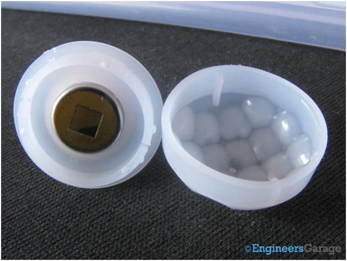
Fig. 4: Internal Set up of PIR Sensor
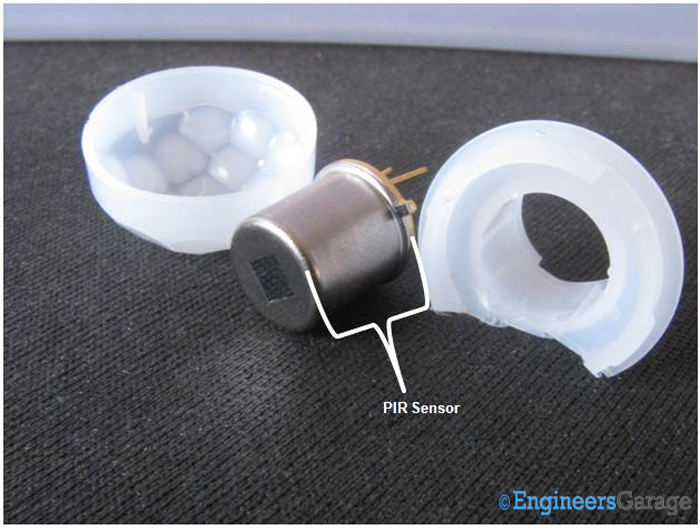
Fig. 5: Shape and Structure of PIR Sensor
The Fresnel array loaded cap is tightly placed over the base region of the plastic molding. There is, however, no latch mechanism to hold it, making it curious to lever the Fresnel lens array out from the plastic assembly. Beneath the Fresnel lens array is the PIR sensor which is firmly placed in the plastic moldings. Placement of the sensor is crucial as it supposed to receive maximum amount of infrared radiation that comes from the lens array. It is hence placed in the center of the moldings where maximum radiation is converged to drop on.
IR Filter & TO5 Metal Can
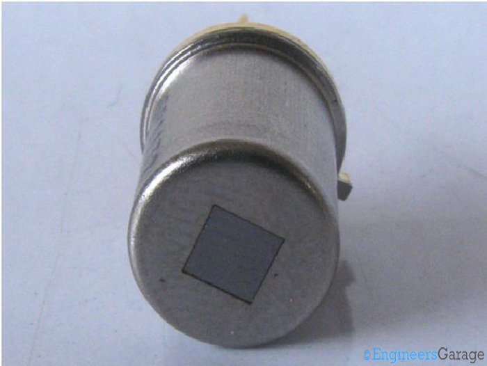
Fig. 6: Infrared Filter of Sensor
At the top of the sensor is the infrared filter. Looking more like a square shaped glass, this filter selects the desired wavelength at which sensor is desired to respond. Since this sensor is designed to detect human presence, the wavelength chosen is 8micrometer to 14 micrometer which is the range within which human body radiates electromagnetic rays.
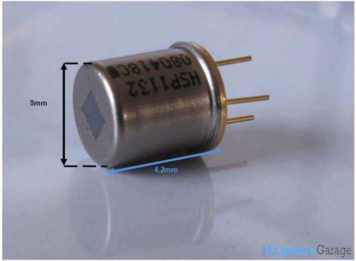
Fig. 7: Design Specifications of Sensor
The body of the sensor is a TO5 metal can structure. TO5 is an industry based standard used for packaging various small modules such as transistors, sensors etc. TO5 metal casing prevents the internal circuitry from external influences such as vibrations or noises which can disturb the normal working of the circuit.
Sensing Element & Chip
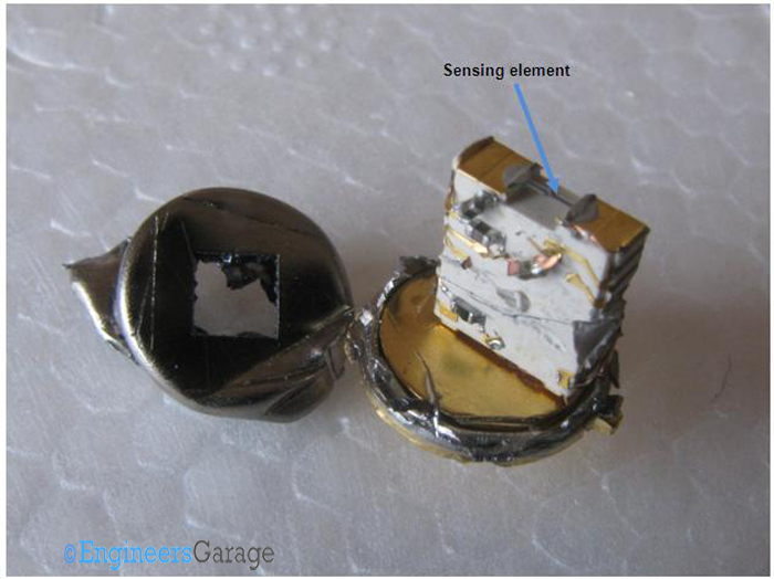
Fig. 8: PCB of PIR Sensor
Uncapping the sensor shows a small PCB which hosts the sensing module, amplifier and a comparator circuit. Image 09 shows the top part of the PCB where the sensing element is placed. Sensing elements are typically made from ferroelectric ceramic (contains lead) or lithium tantalite (lead free). In order to increase the signal receptivity power, multiple sensing elements are taken. The sensor is a quad type and has 4 sensing elements connected in an array.
The IR rays, after passing through the filter, strike this sensing element which generates a charge. The magnitude of the charge produced is directly proportional to the amount of rays that fall on the element.
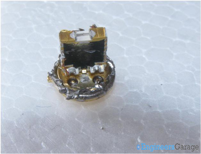
Fig. 9: Amplifier and Comparator of PCB
After the charge gets developed, it is passed onto the amplifier circuitry from which it gets transmitted to the comparator. Further embedded in this PCB are the amplifier and comparator. Previously, these two circuits were included in the external circuitry; however, including them in the sensor module makes the circuit more compact. Since these two circuits are already pre-defined for the IR radiation spectrum, the results tend to be more accurate and precise.
Comparators are used in those sensor modules which give a digital output, like the one here.
FET and Leads
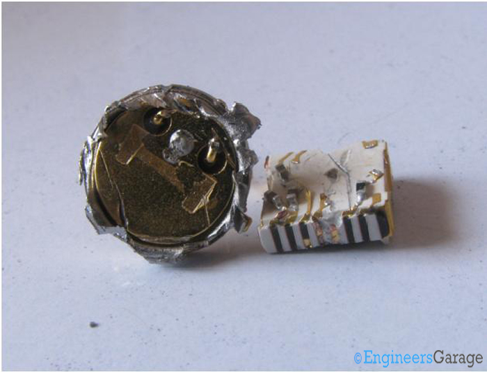
Fig. 10: Base Plate and its Components
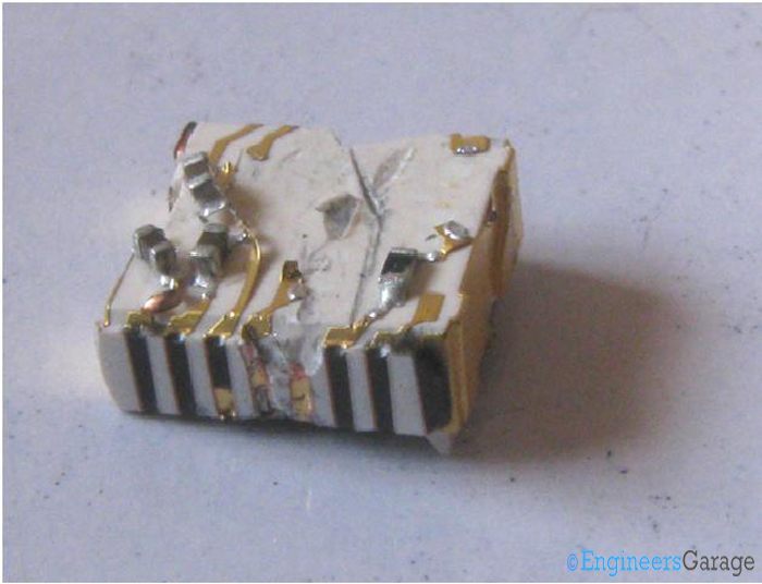
Fig. 11: Processor Unit and Iembedded Resistors
The base plate and the remaining structure of the sensor is a Field Effect Transistor, FET. Even though the charge produced gets amplified, it still manages to generate voltages only of the order of 1mV. FETs can work at such low voltage and can easily transmit the voltage to the processor unit through which the sensor is attached.
Image 10 details with the base plate while image 11 shows the processor unit with a few resistors on it.
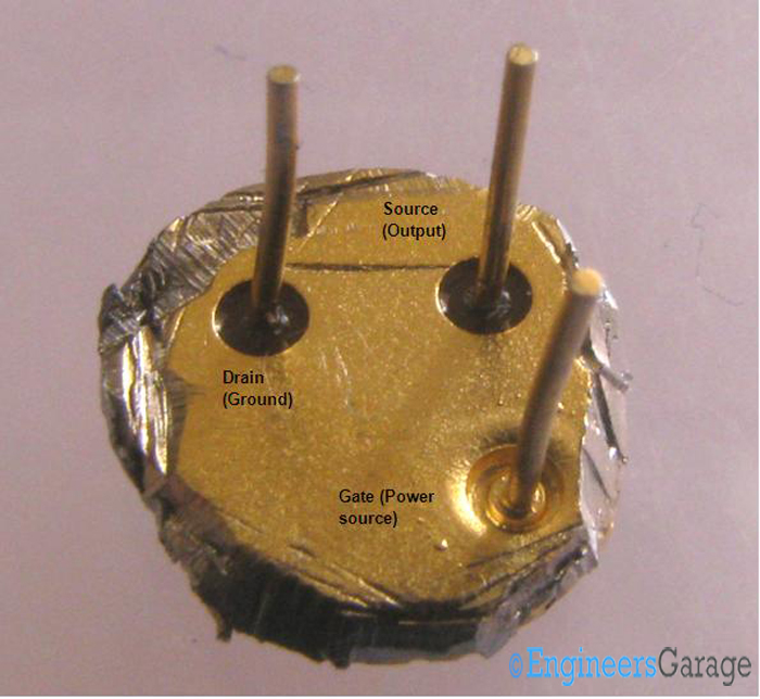
Fig. 12: Multi-functional Connecting Leads of PIR Sensor
At the bottom of the sensor lie, as one would expect, the connecting leads. In this sensor, they perform multitasking: allowing the sensor to be soldered, taking care of small power requirements and sending output to the processing unit.
Image12 shows details of the connecting lead placement which are arranged in the same fashion as in a JFET. The specific function of each lead is shown in the image.
Filed Under: Insight


Questions related to this article?
👉Ask and discuss on Electro-Tech-Online.com and EDAboard.com forums.
Tell Us What You Think!!
You must be logged in to post a comment.