CD4033 is a Johnson counter IC commonly used in digital display. It has a 5 stage Johnson decade counter with decoder which convert the Johnson code to a 7 segment decoded output. Means it will convert the input into numeric display which can be seen on 7 segment display or with the help of LED’s.
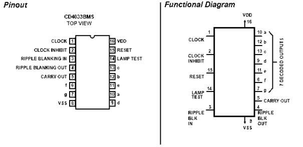
Advantage of this IC is it can be operated at high voltage of 20V. But is highly sensitive, can detect emf present in the atmosphere and is sensitive to static charge also. When you touch your finger at its input terminal its counter get started therefore care should be taken while using it. It can be used in various application like in 7 segment decimal display circuit, in clocks, timer etc. To understand its working first have a look on its pin diagram.

Now let us understand the working of individual pins-
1. Pin 1 known as Clock in – It receives clock signals, and at every positive clock counter advances one by one. You can provide clock with the switch, 555 timer or with the help of logic gates.
2. Pin 2 known as Clock inhibit – CD4033 counter advances one by one by receiving positive pulse at this time clock inhibit pin should be grounded. If it is connected to supply than counter advancement will be inhibited means there will be no meaning of clock pulse.
3. Pin 3 and pin 4 known as Ripple blanking in and Ripple blanking – It is used to display only one zero blanking the other zero. For this IC have ripple blanking in and ripple blanking out. For example you want to display 345 and you are using five 7 segment display then it will display 00345 if blanking input and out is off. But if it is on than you will receive 345. It improves the readability of the circuit.
4. Pin 5 known as carry out – It is used to complete one cycle for every 10 clock input cycle and it also used to cascade more IC’s.
5. Pin 6, pin7 and Pin9 to pin 13 – These are 7 decoded output from a to g used to illuminates the corresponding segment of 7 segment display to display the digit from 0 to 9.
6. Pin 14 known as Lamp test – t is used to check that all segments of 7 segment is working properly or not. For testing momentarily make the pin low.
7. Pin 15 known as Reset – It is used to reset the counter. When it receives high it clears the counter and counting again starts from zero. One important thing reset pin should again made low to start the counter once again.
8. Pin 8 known as ground pin and Pin 16 known as Vdd it should be connected to power supply.
Now let’s understand its working with the help of some example-
1. Interfacing CD4033 with LED’s
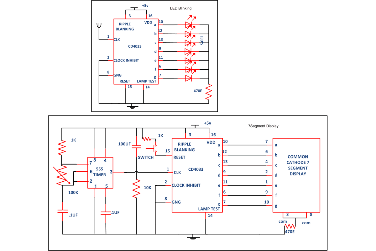
Below circuit can be used to detect the electromagnetic radiation or emf present around it. The radiation may from TV, computer etc.
Working of circuit is simple whenever it detects radiation it receive clock at pin put 1 and its counter starts and LED’s connected at output stars glowing. And the cycle repeats till the reset pin receives high at its input.
2. Interfacing CD4033 with 7 segment display
The circuit describes below count numbers from 0 to 9 and display the same on 7 segment display.
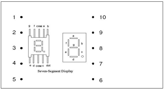
Whenever you press the switch, clock input receives the signals and its counter advances one by one. And it will count up to 9 and again start counting from 0 on each successive pressing of switch. Pin configuration of 7 segment display can be obtained from the fig. shown below.

3. Interfacing CD4033 with the timer IC
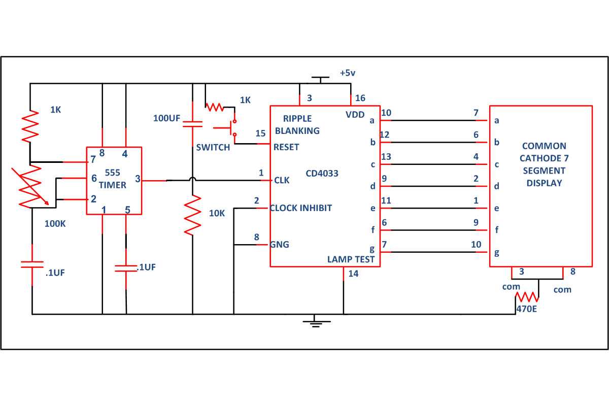
In the following circuit we have used a 555 timer in astable oscillator mode to provide clock signal to input of IC CD4033 to start its counting which can be display on 7 segment display. Here reset switch is used to reset the counting any time needed by the user.
You can also interface two CD4033 IC if you want to increase the counting beyond 9. This can be done by cascading 2 CD4033 IC, connect the carry out of first IC to the clock input of second IC. Now when first IC completes its counting than second IC will start the counting. Connect reset pin of both the IC together and ground it with the help of resistor. And make rest connection like done in following circuit. Similarly you can cascade more IC’s.
Now you can perform different experiments and play around this IC like you can add LDR so that it will start its counter when shadow falls on it or you can cascade two or more CD4033 to make timer circuits etc. So start building your own circuit.
Circuit Diagrams
Filed Under: Electronic Projects


Questions related to this article?
👉Ask and discuss on EDAboard.com and Electro-Tech-Online.com forums.
Tell Us What You Think!!
You must be logged in to post a comment.